DAC Data Transmit from DDR Memory on RFSoC Device
This example shows how to transmit waveforms out of the digital-to-analog converter (DAC) that is read from programmable logic (PL) double data rate 4 (DDR4) memory. Using PL-DDR4 memory offers advantages such as the ability to access 4 gigabytes of memory space. This amount of memory can help facilitate applications requiring large waveform transmissions that are not normally feasible with FPGA block random access memory (BRAM). This figure shows the relevant intellectual property (IP) interfaces and connectivity that are used in this design.

This IP design uses a shared-memory region between the Linux® operating system and PL-DDR4 memory. The memory interface uses the processing system (PS) AXI4 master high performance (HP) lines to directly access PL-DDR4 memory such that it can be accessed with reads and writes. A MATLAB® interface enables access to this shared memory region. This figure shows the flow of the data.

In this figure, the first arrow (labeled 1) shows the moving data over the Ethernet network to the PL-DDR4 memory. The second arrow (labeled 2) shows data that is read from the PL-DDR4 memory to the DAC. The PL design waits on an AXI4 register trigger from MATLAB to initiate data movement and read data out of memory to the DAC.
Requirements
Vivado® Design Suite with a supported version listed in Supported EDA Tools and Hardware
AMD® Zynq® UltraScale+™ RFSoC ZCU111, ZCU208, ZCU216, or DFE ZCU670 evaluation kit.
Open Example
Open the example project and copy the example files to a temporary folder.
1. Navigate to the example source folder by entering these commands at the MATLAB command prompt.
example_root = (hdlcoder_rfsoc_examples_root)
cd (example_root)
2. Copy all of the example files in the DDR4_DACWrite folder to a temporary folder.
Simulate PL-DDR4 DAC Transmit Model
The HDL model for DDR4 DAC transmit is waveformWriteDAC_DDR4.slx. This model simulates the data transfer of using AXI4 master. The waveform that is transmitted can be either an LTE or single-tone waveform, depending on your selection. See the MATLAB script model_init.m.
This figure shows an LTE-transmitted waveform. To synthesize this waveform, you must have the LTE Toolbox™ product. If you do not have this toolbox the waveform that is loaded into memory for the simulation is a 15 MHz complex tone instead.

The waveform in the design is upconverted using interpolation by 4x. The waveform that is stored in memory is 61.44 MHz. Upconvert the data rate to 1966.08 MHz by using a 4x interpolator in the PL device under test (DUT) and the 8x interpolator on the RFSoC. This figure shows a vector interpolator to execute samples and produce a vector of four from a single scalar input.
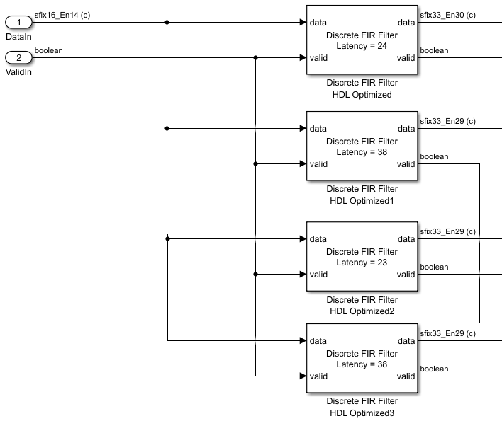
See the subsystem: waveformWriteDAC_DDR4/DDR4_DAC_Transmit/Interpolation_4x/FIR_Vector_Interp. The design also implements the capture logic to collect analog-to-digital converter (ADC) samples using an AXI4-register capture.
Generate HDL and Synthesize Bitstream
Open the model waveformWriteDAC_DDR4.slx, and then right-click the DDR4_DAC_Transmit subsystem. Select HDL Code, then click HDL Workflow Advisor.
In step 1.1 of the HDL Workflow Advisor, select Target platform as Xilinx Zynq Ultrascale+ RFSoC ZCU111 Evaluation Kit, Xilinx Zynq Ultrascale+ RFSoC ZCU208 Evaluation Kit, Xilinx Zynq UltraScale+ RFSoC ZCU216 Evaluation Kit, or Xilinx Zynq UltraScale+ RFSoC DFE ZCU670 Evaluation Kit.
In step 1.2, select Reference design as IQ ADC/DAC Interface.
AXI4-Stream Master data width to
128AXI4-Stream Slave data width to
128Add external memory access (AXI4 Master) to
trueADC sampling rate (MHz) to
1966.08ADC decimation mode (xN) to
8ADC samples per clock cycle to
4ADC mixer type to
FineDAC sampling rate (MHz) to
1966.08DAC interpolation mode (xN) to
8DAC samples per clock cycle to
4DAC mixer type to
FineADC/DAC NCO mixer LO (GHz) to
0.5Enable multi-tile sync to
true
You can set the numerically-controlled oscillator (NCO) mixer frequency to any value and adjust it at run time from MATLAB. If you are using a ZCU208, ZCU216, or ZCU670 board, additionally set the DAC DUC mode parameter to Full DUC Nyquist (0-Fs/2).
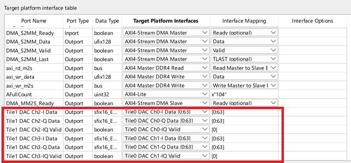
In step 1.3, if you are using a ZCU208 board, for the DAC ports, set the target interface as shown in the image.
In step 4.2, to generate a script that provides MATLAB connectivity to the board for interactive testing and live I/O interfacing, select Generate host interface script and clear the Generate Simulink software interface model checkbox.
Transmit PL-DDR4 DAC Data
After you program the FPGA bitstream, run the script fpgaio_TxWaveformAndCapture.m. The script performs these steps.
Create a complex waveform of size 30.72e5 samples and package the waveform into a data format of
int32.Write the waveform into the PL-DDR4 memory and command the DUT to begin transmitting data over AXI4.
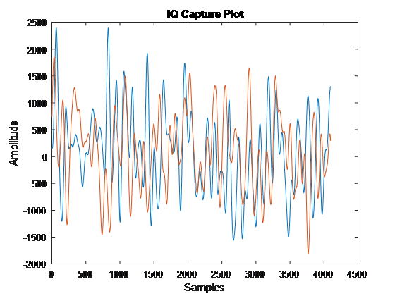
Trigger a data capture of 4096 samples to move ADC data into direct memory access (DMA).
Display the results of the captured ADC data in MATLAB by using this command.
fpgaio_TxWaveformAndCapture
Verify that the data looks as expected by checking an oscilloscope.
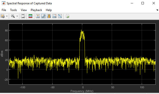
Using an oscilloscope, you can confirm the presence of the waveform by connecting to the correct channel on your RFSoC device and examining the output. For more details on which port to use, check the user guide on SMA cable connectivity. This figure shows an oscilloscope capture of a single tone value that is transmitted out of the DAC channel.
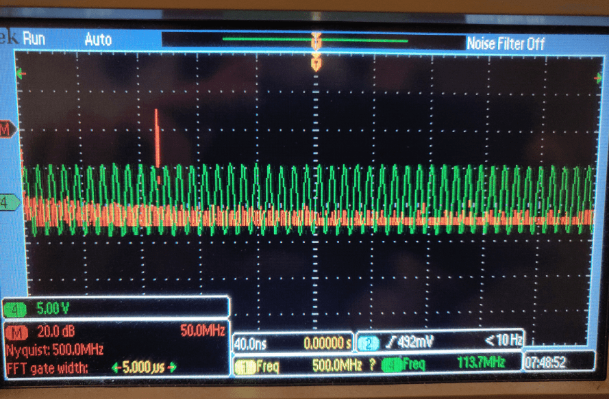
You can choose between the LTE waveform or single NCO tone by adjusting the parameters in the script model_init.m.