Use Synthesis Attributes to Map Adders to DSPs on FPGAs
This example shows how to generate HDL code with synthesis attributes by specifying the SynthesisAttributes HDL block property for a Sum block. During implementation, the synthesis tool maps adders in the Simulink® model to dedicated DSP slices on the FPGA by using the generated HDL code.
The Simulink model in this example targets a Xilinx UltraScale® FPGA, which uses DSP48E2 slices for arithmetic operations. The DSP48E2 slice includes a 27-bit pre-adder, a 27-by-18 multiplier, and a 48-bit accumulator, which enables single-cycle multiply-accumulate (MAC) operations. The slice accepts 30 bits at input A, 18 bits at input B, 48 bits at input C, and 27 bits at input D. The pre-adder adds or subtracts inputs before multiplication. For more information, see the UltraScale Architecture DSP Slice Overview chapter in the Xilinx documentation. You can also run this example on other FPGA devices that provide dedicated DSP units or use different synthesis tools.
Open and Examine the Model
The DUT subsystem of the hdlcoder_mapping_soe_dspe2 model contains a Sum block. To load the model and open the DUT subsystem, enter these commands at the MATLAB® command prompt:
load_system("hdlcoder_mapping_soe_dspe2");
set_param("hdlcoder_mapping_soe_dspe2","SimulationCommand","Update");
open_system("hdlcoder_mapping_soe_dspe2/DUT");
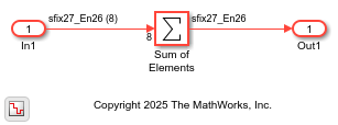
To optimize the adder mapping to a DSP48E2 slice, the model sets Inport block signal width is 27 bits or less. The Sum of Elements block uses these parameter settings:
List of signs is
+.Output data type is
Inherit: Same as first input.Accumulator data type is
Inherit: Inherit via internal rule.
Specify Synthesis Attributes
To map the adder in a Simulink model to a DSP48E2 slice, you specify the synthesis attributes. In this example:
1. Right-click the Sum of Elements block. To add the HDL Coder app options to the context menu, point to Select Apps and click HDL Coder.
2. Right-click the Sum of Elements block. In the HDL Coder section of the context menu, click HDL Block Properties.
3. Next to SynthesisAttributes, click Edit.
4. Set Attribute Name to use_dsp and the Attribute Value to yes.Then, click OK.
For more information about specifying synthesis attributes, see SynthesisAttributes.
Generate HDL Code, Perform Synthesis, and View Resource Report
To generate HDL code, perform synthesis, and view the resource report for the model, use the HDL Workflow Advisor. This example uses Xilinx® Vivado®. To set the tool path, use the hdlsetuptoolpath function to point to an installed Xilinx Vivado executable.
Follow these steps to generate HDL code, perform synthesis, and view the resource report using the HDL Workflow Advisor:
1. In the HDL Code tab, click Workflow Advisor.
2. In HDL Workflow Advisor, in the left pane, Select 1. Set Target > 1.1 Set Target Device and Synthesis Tool, set:
Target workflow to
Generic ASIC/FPGASynthesis tool to
Xilinx VivadoFamily to
Virtex UltraScale+Device to
xcu200-fsgd2104-2-ePackage to
ffg1761Speed to
-2
3. Select 1.2 Set Target Frequency, and set Target Frequency (MHz) to 500.
4. Select 2.1 Check Model Settings. Configure the code generation settings as needed.
5. To generate HDL code, right-click the 3.2. Generate RTL Code task, and select Run to Selected Task.
This code shows the synthesis attributes that HDL Coder generates.
LIBRARY IEEE;
USE IEEE.std_logic_1164.ALL;
USE IEEE.numeric_std.ALL;
USE work.DUT_pkg.ALL;
ENTITY DUT IS
PORT( clk                         :   IN    std_logic;
reset                             :   IN    std_logic;
clk_enable                        :   IN    std_logic;
In1                               :   IN    vector_of_std_logic_vector27(0 TO 7);  -- sfix27_En26 [8]
ce_out                            :   OUT   std_logic;
Out1                              :   OUT   std_logic_vector(26 DOWNTO 0)  -- sfix27_En26
);
END DUT;
ARCHITECTURE rtl OF DUT IS
ATTRIBUTE use_dsp : string;
ATTRIBUTE use_dsp OF Sum_of_Elements_op_stage1 : SIGNAL IS "yes";
ATTRIBUTE use_dsp OF Sum_of_Elements_op_stage2 : SIGNAL IS "yes";
ATTRIBUTE use_dsp OF Sum_of_Elements_op_stage3 : SIGNAL IS "yes";
ATTRIBUTE use_dsp OF Sum_of_Elements_op_stage4 : SIGNAL IS "yes";
ATTRIBUTE use_dsp OF Sum_of_Elements_op_stage5 : SIGNAL IS "yes";
ATTRIBUTE use_dsp OF Sum_of_Elements_op_stage6 : SIGNAL IS "yes";
ATTRIBUTE use_dsp OF Sum_of_Elements_out1 : SIGNAL IS "yes";
...
6. In the left pane, navigate to 4. FPGA Synthesis and Analysis > 4.2 Perform Synthesis and P/R > 4.2.2. Run Implementation. Clear Skip This Task.
7. Right-click 4.2.2 Run Implementation and select Run to Selected Task.
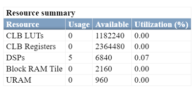
After synthesis and implementation, you can view the Resource Summary section in the Result pane. This resource summary table shows the number of adders that the tool maps to DSP slices. In this example, the synthesis tool uses five DSP slices.
For more information on code generation and synthesis steps, see HDL Code Generation and FPGA Synthesis from Simulink Model.