Current-Programmed Mode Controller Design for Point-of-Load Buck Converter
R2026bThis example shows how to design a controller with a current- programmed mode (CPM) inner loop for a point-of-load (PoL) switched mode power supply (SMPS) buck converter using Mixed-Signal Blockset™ operating point analysis to generate a small signal model and controller tuning from Control System Toolbox™.
Power supplies which perform the voltage regulation for a high power digital processor such as the GPUs or ASICs central to an AI data center infrastructure are commonly called point-of-load converters because the digital processor is the primary load for the power supply, and so the power supply is placed close to its load. In this application the processor typically switches abruptly between standby and active modes, producing very large load current steps with extremely short rise/fall times. The PoL voltage regulator must respond to these load current steps with minimum variation in output voltage.
PoL voltage regulators are usually designed with an inner CPM control loop and an outer voltage control loop. The CPM loop damps the resonant behavior of the power train, increasing the stability and bandwidth of the voltage control loop. The Loop Gain Calculation for Current-Programmed Mode Control of Switched-Mode Power Supplies document [1] provides simple mathematics that enables engineering insight and makes it easy to choose the optimum CPM loop gain.
Because they regulate current, CPM loops are also used to make sure that multiple half bridges in parallel share current equally. In this application there is usually a separate switch cycle phase for each half bridge.
This example implements the design calculations for both the CPM and voltage control loops, applies them to the detailed design of a 12V to 1V PoL regulator with a 100A nominal output current, and uses a Simulink™ behavioral model to demonstrate the regulator's response to abrupt load current steps from 0A to 70A to 100A and back again. The regulator completely responds to an abrupt 70A to 100A load step within eight switching cycles, with a maximum voltage deviation of 60mV.
Dual Loop Voltage Regulator
The following figure is a simplified schematic for a dual loop voltage regulator.
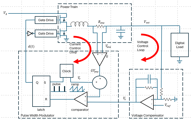
In this circuit an inductor current sense resistor in the power train is connected directly to the pulse width modulator (PWM), forming a current programmed mode (CPM) control loop. When the sensed current becomes greater than a current threshold set by the Vc control voltage, the PWM latch is reset, causing a falling edge in the PWM output. The falling edge switches the transistors so that the inductor is connected to the return node instead of the supply voltage Vg, causing the inductor current to decrease rather than increase. [1] provides a detailed description and mathematical analysis of the CPM control loop.
The voltage compensator senses voltage Vout delivered to the digital load and produces the control voltage Vc, thus incorporating the power train and PWM into a voltage control loop. When Vout falls below the value set by the reference voltage and voltage compensator, the compensator increases Vc, thus increasing the current delivered by the power train and increasing Vout.
PoLPowerSupplyPDNload is a Simulink time domain model of the dual control loop structure.
sysmdl = "PoLPowerSupplyPDNload";
open_system(sysmdl);
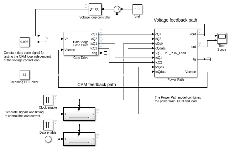
In this model the power train and digital load are modeled in the Power Path block while the PWM and gate drives are modeled in the Gate Drive block. The Gate Drive block includes a 75ns transistor turn-on dead time but does not model the detailed interaction between the gate drive and the transistor in the power train.
The Vsense output of the Power Path block is fed back to the Vsense input of the Gate Drive block, completing the CPM control loop.
The Vref, summing junction and Voltage loop controller blocks model the voltage compensator circuit. The Vout output of the Power Path block is fed back to the summing junction, and the output of the Voltage loop controller block is fed back to the Gate Drive block, completing the voltage control loop.
The Clock enable and Data enable signals control the state of the digital load. When Clock enable and Data enable are both zero, the digital load is off. When Clock enable is one and Data enable is zero, the digital load is in standby state (70 amps DC), and when both signals are one the digital load is active (100 amps DC).
Digital Load Model
The digital load modeling in this example assumes that the digital processor is a very large CMOS logic design with a single high frequency clock, and that at any one time the entire processor is either in standby or active mode. This is a simplification in that many digital processors have multiple clock domains whose operational modes do not necessarily depend on each other. In that sense, modeling mode transitions as always involving the entire processor is a worst case assumption.
The current drawn by a CMOS logic design depends on the parasitic capacitances distributed throughout the design, the clock frequency, the percentage of gates switching in any one clock period, and the power supply voltage (Vdd). Consider the simple case of one inverter driving another inverter:
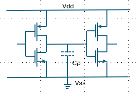
There is a parasitic capacitance Cp attached to the input inverter's output.This capacitance is a combination of the transistor gate capacitances for the output inverter plus routing capacitance of the traces connecting the two inverters.
When the input inverter switches its output state from zero to one the Cp is charged to the power supply voltage Vdd and when it switches its output state from one to zero the charge on Cp is conducted to the return node Vss. The result is that a switch to one and back to zero consumes a charge of Q = Vdd*Cp from the power supply.
If in an average clock cycle the equivalent of Ng of these charge transfers are completed, and the clock frequency is Fc, then the average current is I = Vdd*Cp*Ng*Fc. This average current is the current that would be consumed by a resistor with a value Rl = 1/(Cp*Ng*Fs).
In normal operation the exact number of logic transitions that occur in each clock cycle will vary. However that variation tends to be independent from one clock cycle to the next, and so in addition to the DC current consumption the load current will have a white noise component (called a stochastic process) similar to shot noise, only on a much larger scale. However the amplitude of that noise component will be proportional to the square root of Ng whereas the DC current will be proportional to Ng, and so the white noise amplitude will be much smaller than the DC current.
In any one operational mode (off, standby, active) this example models the DC portion of the load current and does not include the stochastic current variation. However this average current is assumed to change when the operation mode changes.
The time it takes the average current to change when the operational mode changes is also well understood. Consider that no practical logic design can complete the processing of any specific piece of data in a single clock cycle. Rather, the data processing is broken into stages that can be reliably completed in one clock cycle, and these stages are organized in what is called a pipelined logic design, as shown below.
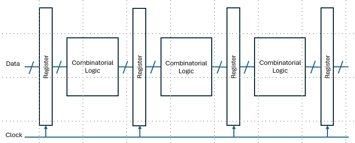
Each processing stage is implemented by combinatorial logic gates (AND, OR, NAND, NOR, inverter), and the output of each stage is stored in a register so that in the next clock cycle it can become the input to the next stage. It is common to have tens of pipeline stages in a logic design.
To transition from one operational mode to the next, either data has to be input into one end of the pipeline and make its way to the other end, or else the data that is already in the pipeline needs to make its way to the output. Either way, a mode transition will require about as many clock cycles as there are stages in the pipelined logic design.
Even so, the current transient due to an operational mode change can be very rapid compared to the switching frequency of an SMPS. Processors often have clock frequencies of the order to 2GHz, so it is common for mode transitions to occur in tens of nanoseconds.
The time domain model in this example uses a sample time of 20ns, and applies the mode transitions in a single sample interval. This transition time should be considered realistic.
Power Train Small- Signal Model
The circuit design of the power train for this example is a buck topology driven by a half bridge transistor network, as described in detail in the Power Train Output Ripple Due To Parasitic Inductances example [2]. However the CPM loop design mathematics uses a discrete time (Z domain) control matrix model with a sample time equal to the switching period. To be valid for CPM loop design, the small signal model for the power train must be derived from an equivalent circuit whose poles do not exceed the Nyquist frequency associated with the power train switching frequency.
The equivalent circuit used in this example is identical to that used in [2] except that the parasitic inductances have been omitted to remove their high frequency poles.
open_system("PoLPowerTrain");
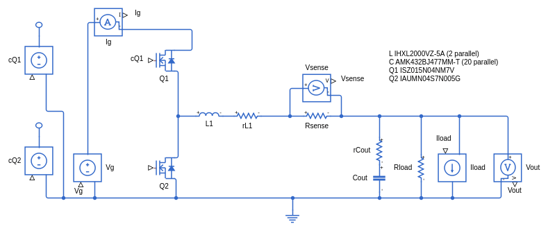
As explained in the previous section Rload is used to model the digital load.
For the initial small signal model the load resistance was set to 0.01Ω, consistent with the nominal 1V, 100A operation of the voltage regulator. The analysis can be repeated with other load resistance values to reflect the activity at other operating points.
Iload is set to zero and used only as an input with which to evaluate the power train's output impedance.
Use operating point analysis to create the small signal model for the power train.
In the following code the PhaseOffsets name/value expression causes the switching cycle to start ("0") with the falling edge driven by the CPM loop and then places the rising edge ("1-d") one duty cycle away from the end of the switch cycle. The PulseDuration name/value pair includes a 75ns turn-on delay scaled to the length of the switch cycle ("-75e-9*1e5"). The turn-on delay is required for a transistor half bridge circuit.
set_param("PoLPowerTrain/Rload","R","0.01");
set_param("PoLPowerTrain/Rload","R","0.01");
cktobj = cktconfig("PoLPowerTrain",...
    Ports = {"cQ1","cQ2","Vg","Iload","Vout","Ig","Vsense"},...
    CircuitDesignName = "Buck",...
    BlockName = "Power Train");
[dcResults,~,waves,ssmodels,abcd,~] = cktoperpoint(cktobj,...
    OutputPort = "Vout",...
    OutputValues = 1,...
    InputValues = {"Vg" 12;"Iload" 0},...
    ControlVariable = "Duty cycle",...
    DutyCycle = [0.05 0.5],...
    Frequency = 1e5,...
    PhaseOffsets = '[1-d,0]',...
    PulseDuration = '[d-75e-9*1e5,1-d-75e-9*1e5]',...
    WaveSamples = 1024);

Construct a map from the circuit elements to the circuit nodes, to support interpretation of the waves output.
circuittable = ckttbl(cktobj);
disp(circuittable);
    Designator      Value       Positive    Negative    Current Node    Control+    Control-          Type
    __________    __________    ________    ________    ____________    ________    ________    ________________

     "cQ1"        "cQ1"          "V5"        "V0"         ""             ""            ""       "Voltage input"
     "cQ2"        "cQ2"          "V4"        "V0"         ""             ""            ""       "Voltage input"
     "Vg"         "Vg"           "V2"        "V0"         ""             ""            ""       "Voltage input"
     "Iload"      "Iload"        "V0"        "V6"         "Iload"        ""            ""       "Current input"
     "Vout"       "Vout"         "V6"        "V0"         ""             ""            ""       "Voltage output"
     "Ig"         "Ig"           "V2"        "V9"         "Ig"           ""            ""       "Current output"
     "Vsense"     "Vsense"       "V7"        "V6"         ""             ""            ""       "Voltage output"
     "Cout"       "0.006554"     "V1"        "V0"         ""             ""            ""       "Capacitor"
     "L1"         "2.35e-07"     "V3"        "V8"         "iL1"          ""            ""       "Inductor"
     "Q1"         "0.00155"      "V9"        "V3"         "ivbdQ1"       "cQ1"         ""       "MOSFET"
     "rdsQ1"      "1"            "vdQ1"      "V9"         ""             ""            ""       "Resistor"
     "vbdQ1"      "0"            "V3"        "vdQ1"       "ivbdQ1"       ""            ""       "Voltage source"
     "Q2"         "0.0005"       "V3"        "V0"         "ivbdQ2"       "cQ2"         ""       "MOSFET"
     "rdsQ2"      "1"            "vdQ2"      "V3"         ""             ""            ""       "Resistor"
     "vbdQ2"      "0"            "V0"        "vdQ2"       "ivbdQ2"       ""            ""       "Voltage source"
     "Rload"      "0.01"         "V6"        "V0"         ""             ""            ""       "Resistor"
     "Rsense"     "0.0001"       "V7"        "V6"         ""             ""            ""       "Resistor"
     "rCout"      "5e-05"        "V6"        "V1"         ""             ""            ""       "Resistor"
     "rL1"        "0.000105"     "V8"        "V7"         ""             ""            ""       "Resistor"
The open loop small signal model is expressed as a Control System Toolbox ss object in the ssmodels output and as a set of control matrices in the abcd output. The CPM loop analysis is performed using the control matrices.
The dcResults and waves outputs are used to derive some of the parameters used in the CPM loop analysis.
CPM Loop Design
The goal of CPM loop design is to choose a loop gain that will move the CPM closed loop poles away from the Laplace domain imaginary axis (oscillating behavior) to the Laplace domain real axis (damped behavior) without moving any pole closer than necessary to the origin (slow behavior).
The approach presented in this example is to calculate the CPM poles as a function of gain, present them in a table, and manually choose the gain from the table.
In [1] the closed loop solution for the CPM duty cycle variations and the state equation when that solution is inserted into the small signal model control matrix equation are

where  is the control voltage,
  is the current sense voltage,
  is the ramp slope,
  is the CPM loop gain,
  is the slope of the sensed current and
  is the switch period.
Note in particular that the CPM loop ends up directly modulating the inductor term in the A matrix.
Use dcResults and waves to determine the waveform slopes needed in the CPM analysis.
wavetable = waves{1};
vsense = wavetable.V7 - wavetable.V6;
D = dcResults{1,"Duty Cycle"};
Ts = abcd(1).tau;
mvsns = (max(vsense)-min(vsense))/(D*Ts);
ma    = 1/Ts;
Gmax  = (1-D)/(max(vsense)-min(vsense));
Use abcd to partition the control matrices in a way that separates the response to the duty cycle input and current sense output from the response to the rest of the inputs and outputs.
ASSUMPTIONS
1. The duty cycle control is the last input in the vector of inputs to the small signal model.
2. The voltage from the current sense resistor is the last output of the small signal model.
A = abcd(1).A;
B = abcd(1).B;
C = abcd(1).C;
D = abcd(1).D;
[~,ni] = size(B);
no   = size(C,1);
Bss1 = B(:,1:ni-1);
Bss2 = B(:,ni);
Css1 = C(1:no-1,:);
Css2 = C(no,:);
Dss1 = [D(1:no-1,1:ni-1) zeros(no-1,1)];
Compute and display the table of closed loop poles as a function of CPM loop gain.
Garray = [0 5 10 12 14 16 18 20 30];
poletable = cpmctpoles(Garray,A,Bss2,Css2,Ts,ma,mvsns);
disp(poletable);
    Gain        Pole_1            Pole_2
    ____    ______________    ______________

      0     -11746+22243i     -11746-22243i
      5     -22264+20185i     -22264-20185i
     10     -29644+14630i     -29644-14630i
     12     -32015+11350i     -32015-11350i
     14     -34132+6570.8i    -34132-6570.8i
     16     -42474+0i         -29598+0i
     18     -48898+0i         -26613+0i
     20     -53614+0i         -25021+0i
     30     -69077+0i         -21675+0i
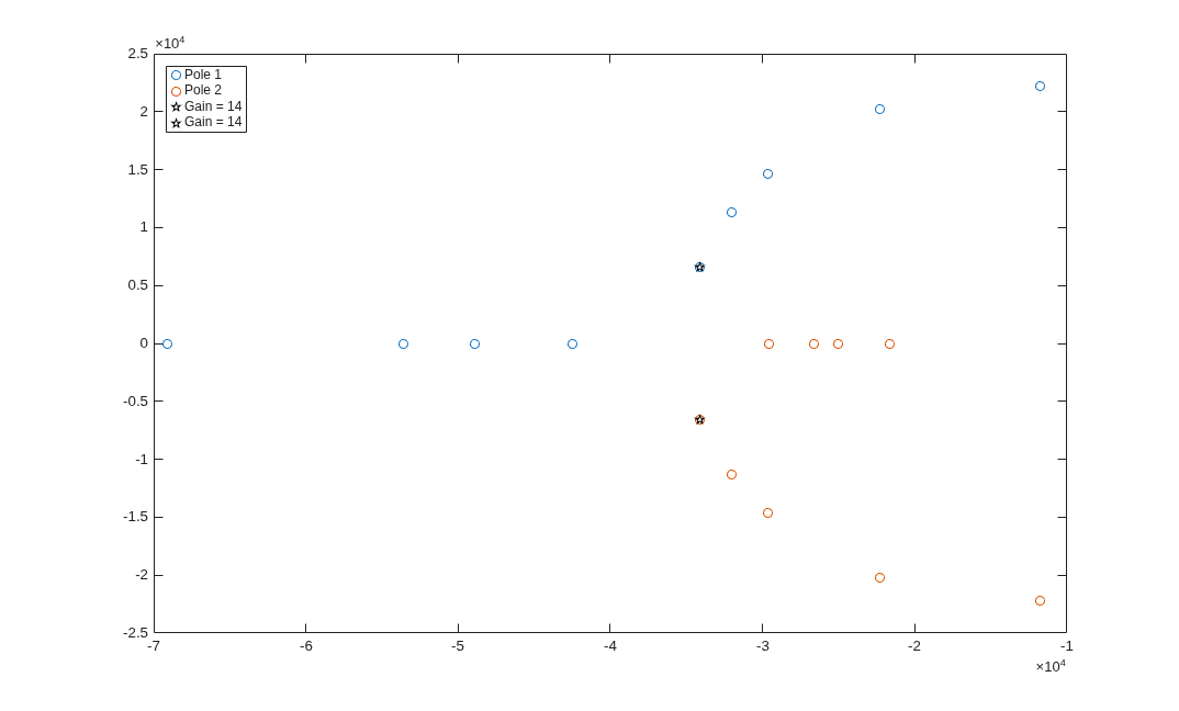
From the table it appears that a gain of 14 will bring the poles almost to the real axis while a gain of 16 will bring them both to the real axis and separate them, increasing the magnitude of one pole while reducing the magnitude of the other. Either gain would be a reasonable choice, and a gain of 15 might be slightly better. However near the optimum gain, the loop behavior is relatively insensitive to the precise value. For this example choose a gain of 14.
Plot the CPM loop poles as a function of gain, highlighting the design choice Gain = 14.
figure(6);
plot(poletable.Pole_1,"o");
hold on;
plot(poletable.Pole_2,"o");
plot(poletable.Pole_1(5),"pentagramk");
plot(poletable.Pole_2(5),"pentagramk");
legend("Pole 1","Pole 2","Gain = 14","Gain = 14","Location","northwest");
Create equivalent small signal models for the open loop power train and the as-tuned CPM loop.
Bop = [Bss1 Bss2/(ma*Ts)];
opss = ss(A,Bop,Css1,Dss1,Ts,"InputName",{'Vg' 'Iload' 'Vc'},...
    "OutputName",{'Vout' 'Ig'});
G = 14;
Acpm = A - G/((ma+G*mvsns)*Ts)*Bss2*Css2;
Bcpm = [Bss1 Bss2/((ma + G*mvsns)*Ts)];
cpmss = ss(Acpm,Bcpm,Css1,Dss1,Ts,"InputName",{'Vg' 'Iload' 'Vc'},...
    "OutputName",{'Vout' 'Ig'});
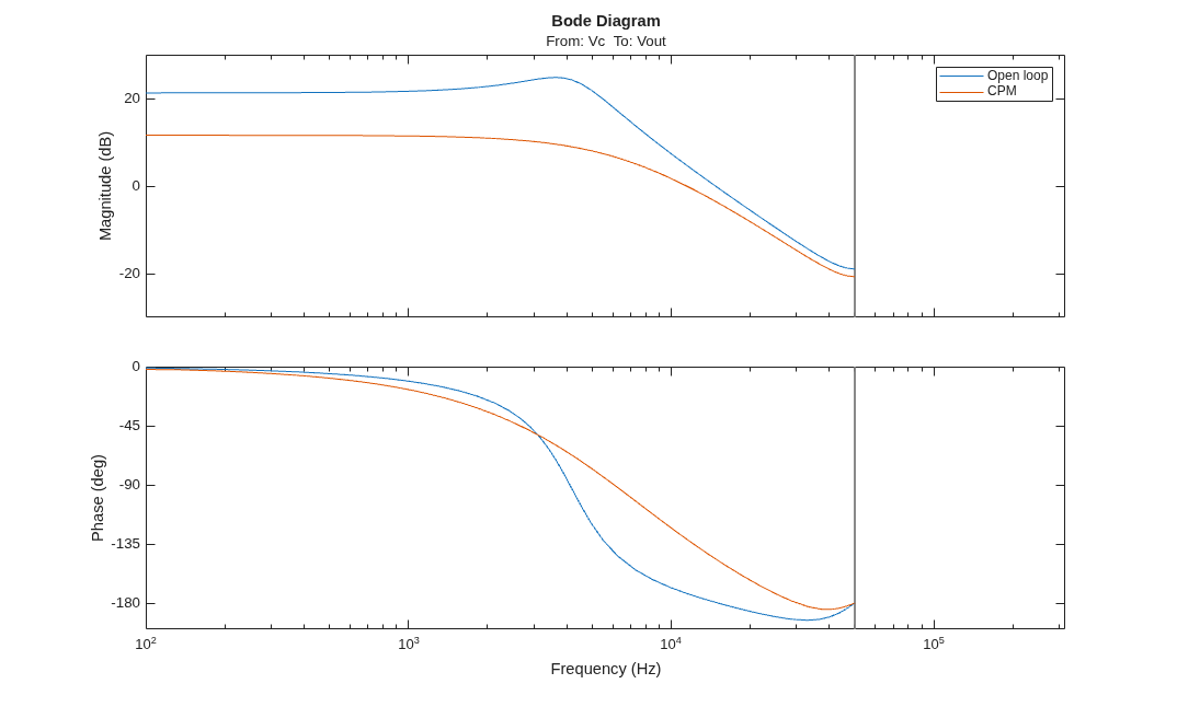
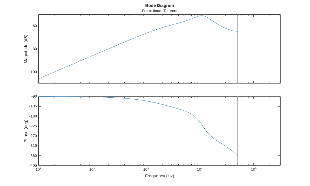
Create Bode plots for the gain of both the power train and the CPM loop, and for their output impedance.
figure(1);
h = bodeplot(opss(1,2),cpmss(1,2));
h.FrequencyUnit = 'Hz';
h.Legend.Visible = "on";
h.Legend.String = ["Open loop" "CPM"];
figure(2);
h = bodeplot(opss(1,3),cpmss(1,3));
h.FrequencyUnit = 'Hz';
h.Legend.Visible = "on";
h.Legend.String = ["Open loop" "CPM"];
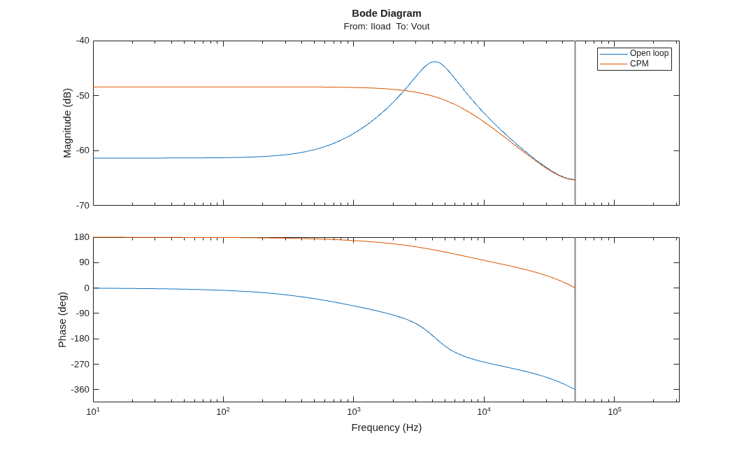
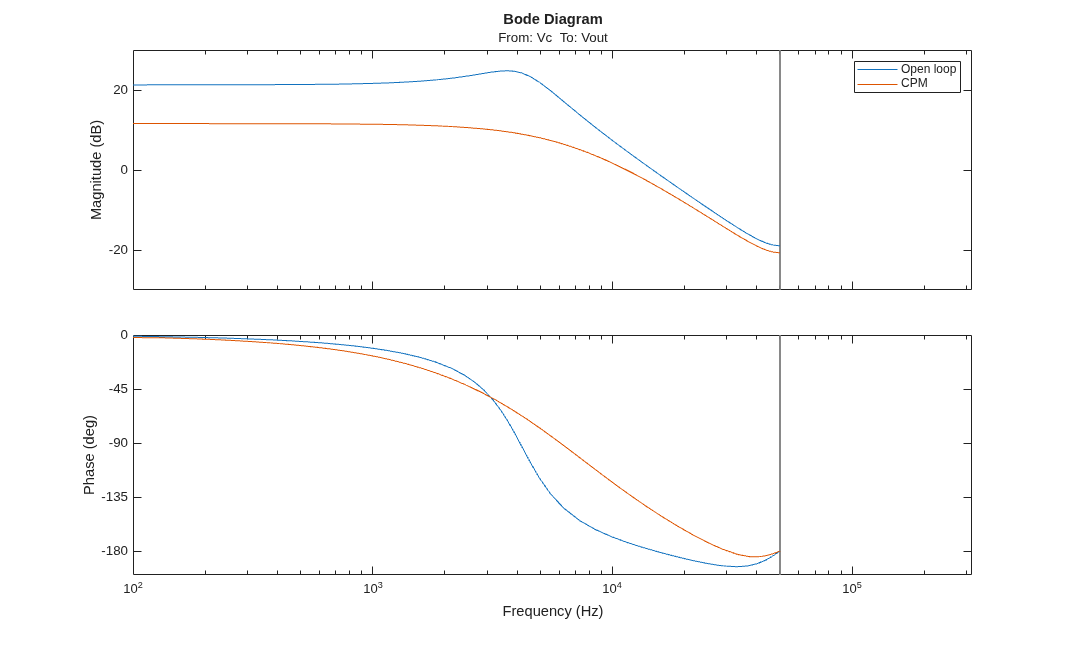
Note that with the CPM loop the control voltage response magnitude varies much more smoothly and the phase changes much more slowly, offering more loop phase and gain margin to the outer voltage control loop.
The open loop power train impedance resembles an inductance at lower frequencies while the CPM loop impedance resembles a capacitor. The current step response of the capacitive impedance will be much more desirable.
Voltage-Control Loop Design
The outer voltage control loop is designed by applying the Control System Toolbox systune function to a PI controller. Note that without the CPM loop a much more complex type III compensator would be required.
The first step is to combine a PI controller (Cntl) with a summing junction (Sm) and the CPM loop (cpmss) into a closed loop control model (Supply).
Cntl = tunablePID('Ct','PI');
Cntl.InputName = 'Verr';
Cntl.OutputName = 'Vc';
Cntl.Ts = cpmss.Ts;

Sm = sumblk("Verr = - Vout");
APs = 'Vout';
Supply = connect(cpmss(1,2:3),Cntl,Sm,'Iload','Vout',APs);
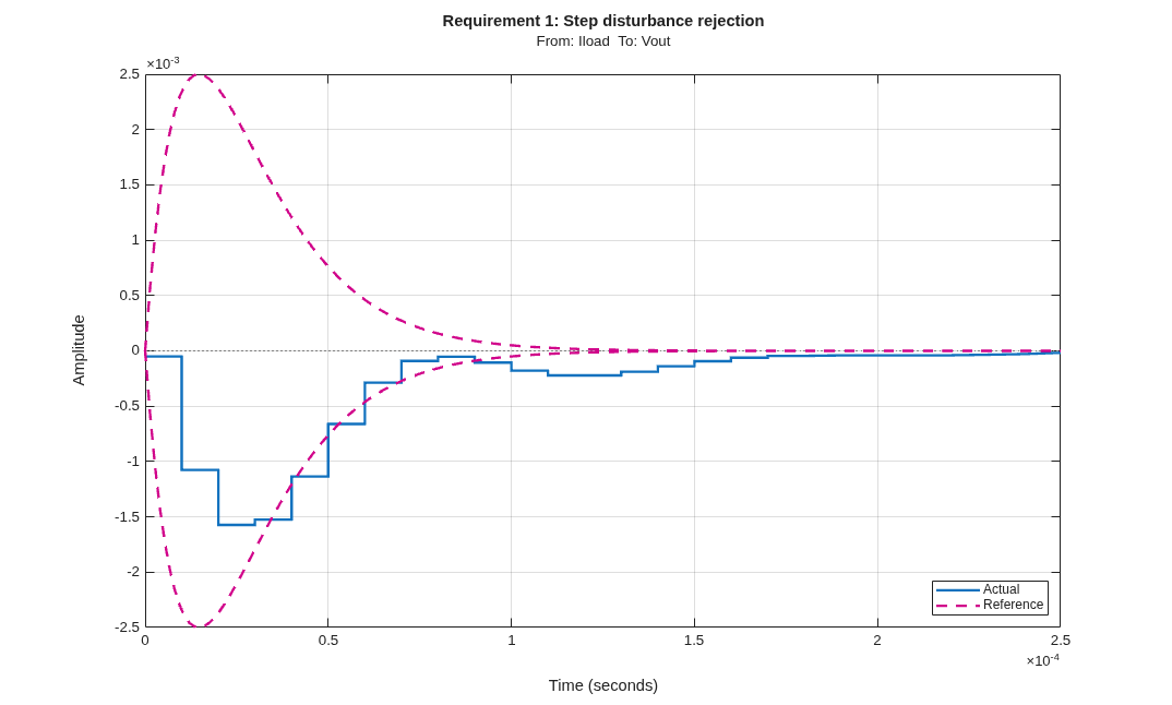
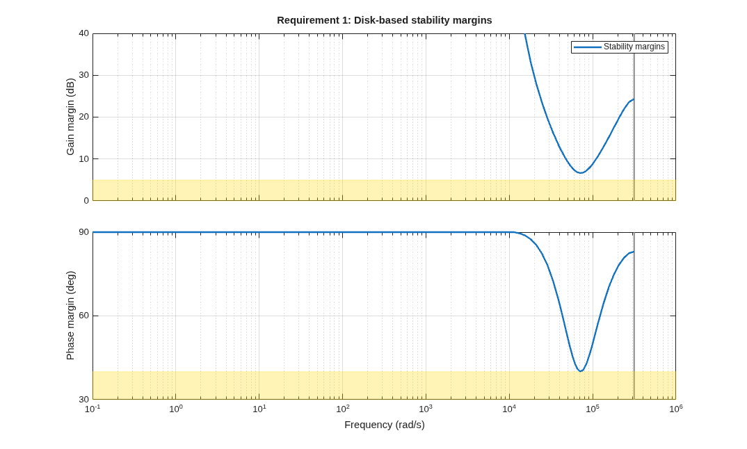
Define the tuning goals. There will be a required ("hard") tuning goal for loop phase and gain margin, and a desired ("soft") tuning goal for current step response.
The hard tuning goal is 5dB gain margin and 40 degrees phase margin.
Rmargins = TuningGoal.Margins('Vout',5,40);
The soft tuning goal is a step response goal with an amplitude and a duration. The values for these parameters are determined by iterating until the scores for both the hard tuning and the soft tuning are about equal to one. First, reduce the duration until the hard tuning goal is met with a score very close to one but with minimal ringing in the tuned step response. Then reduce the amplitude to until the soft tuning score is near one. For this example choose a duration of a tenth of a millisecond and an amplitude of 2.5mV.
Rstep = TuningGoal.StepRejection('Iload','Vout',2.5e-3,0.1e-3);
Apply the Control System Toolbox systune function and extract the tuned PI controller object so that its settings can be inserted into the control loop design and time domain simulation.
SupplyT = systune(Supply,Rstep,Rmargins);
CntlT = getBlockValue(SupplyT,'Ct');
disp(CntlT);
Final: Soft = 0.81, Hard = 0.99861, Iterations = 135
              Ts
  Kp + Ki * ------
              z-1

  with Kp = 0.721, Ki = 1.24e+04, Ts = 1e-05

Name: Ct
Sample time: 1e-05 seconds
Discrete-time PI controller in parallel form.
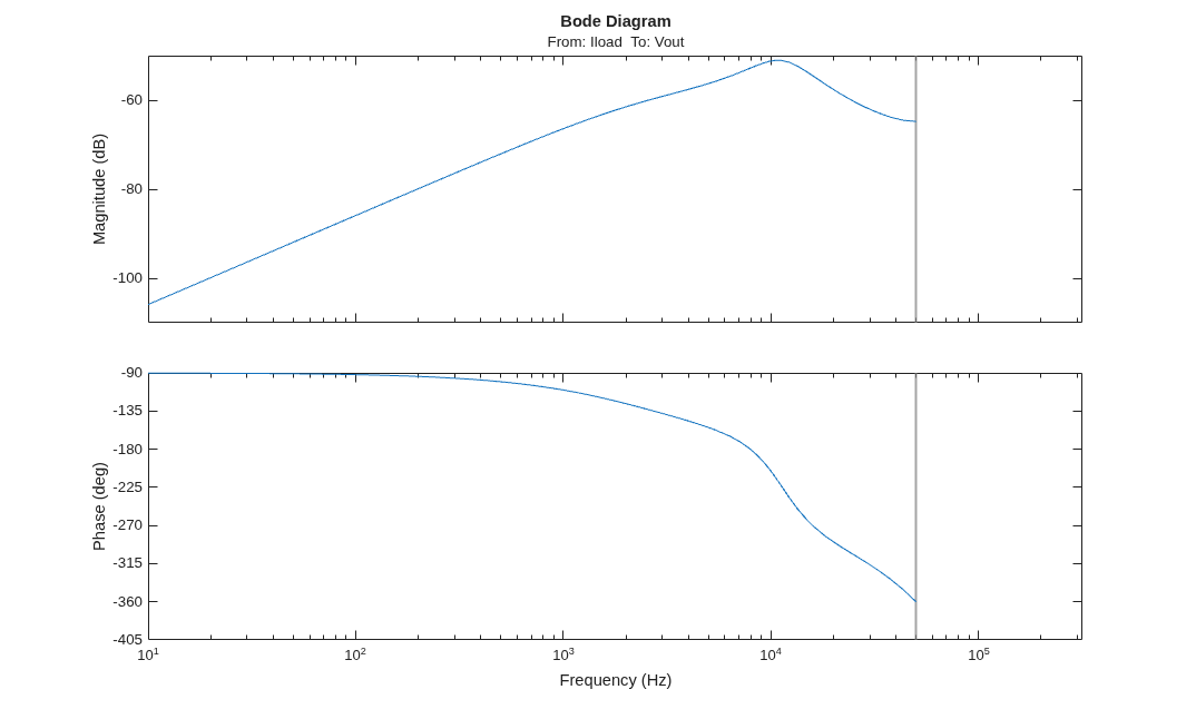
View the degree to which tuning goals were met and the power supply output impedance at this operating point.
figure(3);
viewGoal(Rstep,SupplyT);
figure(4);
viewGoal(Rmargins,SupplyT);
figure(5);
h = bodeplot(SupplyT);
h.FrequencyUnit = 'Hz';
Set the parameters for the voltage control loop in the time domain model.
set_param(sysmdl+"/Voltage loop controller","P",num2str(CntlT.Kp));
set_param(sysmdl+"/Voltage loop controller","I",num2str(CntlT.Ki));
Time-Domain Model
The goal of the time- domain model is to evaluate the current load step response of the completed power supply design at multiple operating points. This requires that the abrupt load step behavior of the digital load is modeled accurately as well as the detailed interaction between the power supply and the load.
A Simulink behavioral modeling approach was chosen to simplify the modeling of the diverse model components and minimize the simulation time.The unidirectional interfaces in this approach require some adaptation in the model structure. For the time domain model in this example the load switching was included in the Power Path circuit block model to isolate the interaction between the power train and the load inside a single block. Also, a linear extrapolation algorithm was included inside the Gate Drive block to compensate for a one sample delay in the CPM loop.
In contrast to the circuit model used to prepare the power train small signal model, the power train circuit model for the time domain simulation includes the capacitor equivalent series inductances (lCout and lCout1) and a simple model of the power plane spreading inductance (Lsprd).
mdl = "PoLPowerTrainPDNload";
open_system(mdl);
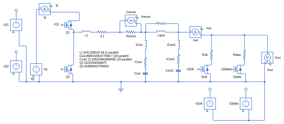
Note that while Cout is an array of 470uF capacitors, Cout1 is an array of 22uF capacitors. Consistent with common design practice, the faster Cout1 capacitors are placed closer to the load. Cout1 has a specific effect that will be observed in the model's step response.
To include the load switching in this circuit Rload has been replaced by transistor controlled resistors. The value for Rclk was chosen to model a 70A current drawn by the digital load's clock distribution network and flip-flops while the Rdata value was chosen to model the 30A current drawn by the combinatorial logic in active mode. In the simulation the digital load will be sequenced from "off" (0A) to "standby" (70A) to "active" (100A) and then back to "standby" and "off". In the simulation the digital load state transitions occur in one sample time of 20ns.
Construct or refresh the power path block in the model:
cktobj = cktconfig(mdl,...
    Ports = {"cQ1","cQ2","cQclk","cQdata","Vg","Vout","Iout","Ig","Vsense"},...
    CircuitDesignName = "PT_PDN_Load",...
    BlockName = "Power Path");
blockpath = cktblock(cktobj,sysmdl);
set_param(blockpath,"InheritSampleRate","off");
set_param(blockpath,"SampleRate","5e7");
Run the model.
simout = sim(sysmdl);
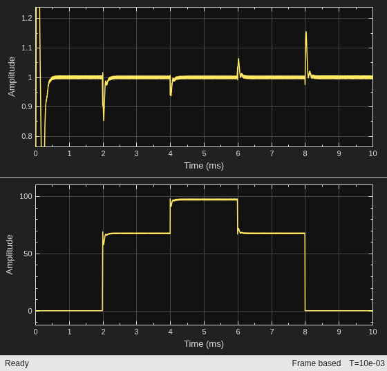
Many of the signals in the model were configured to be logged, including Vout and Iout. You can examine these signals in more detail using the Simulink Data Inspector. You can open the Simulink Data Inspector from the model or use the command line
Simulink.sdi.view;
In the Simulink Data Inspector choose "Power Path 1" to view Vout. You can then examine the transition to standby mode (0A to 70A) and the transition from standby mode to active (70A to 100A) in more detail.
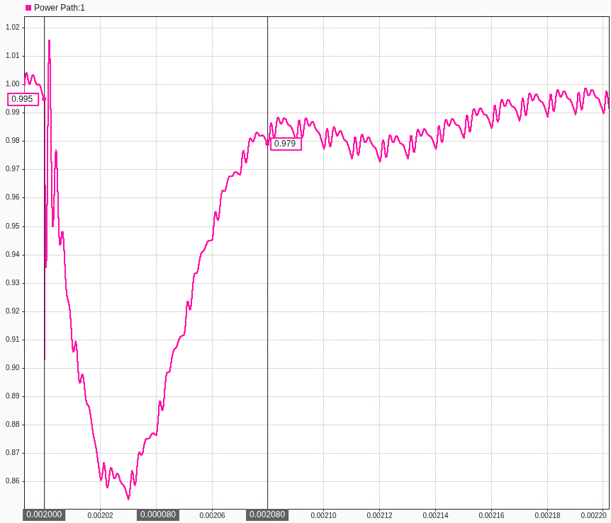
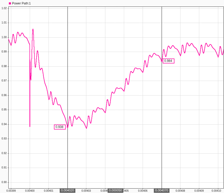
Note in these high resolution views of the step response that there is a distinct one sample spike when the load steps are first applied. This initial spike is controlled by Cout1 before the larger Cout has had time to respond. The count of 18 capacitors in the Cout array was specifically chosen to make the amplitude of this spike equal to the amplitude of the subsequent power supply spike. Less than 18 capacitors produced a larger initial spike that, if large enough, could reset the digital processor before the power supply has had a chance to respond. A count of 20 capacitors produced a much lower amplitude spike but a more distinct parallel resonance between the capacitance of Cout1 and the ESL of Cout.

