DC Power Integrity Analysis of PCB Power Planes
R2026bThis example demonstrates how to use RF PCB Toolbox to perform DC power integrity (PI) analysis on custom power plane geometries. The workflow uses pcbComponent to define plane shapes with realistic anti-pad patterns, and powerDistributionNetwork to solve for voltage distribution, current density, and IR drop under specified load conditions.
DC PI analysis answers the fundamental question: does the power plane deliver adequate voltage to the load under full current draw? Plane geometry — routing slots, anti-pads from signal vias, and copper keep-outs — directly impacts current distribution, IR drop, and peak current density. This example quantifies those effects across multiple geometry variants, providing data for early-stage design decisions.
What this example covers:
Building custom power plane shapes using antenna geometry primitives
Configuring source, load, and sense vias in a
powerDistributionNetworkExtracting and interpreting voltage deviation and surface current density
Comparing IR drop and peak current density across plane variants
Using a solid reference plane to validate solver results
Define Board Parameters and Stackup
The analysis targets a 0.8 V core rail on a 50 mm x 50 mm board region carrying 50 A total load — representative of a modern high-performance ASIC power domain. The stackup is a buried power-ground plane pair separated by 75 um FR-4.
mm  = 1e-3;
mil = 25.4e-6;

boardL = 50*mm;
boardW = 50*mm;

Vnom   = 0.8;                   % Nominal rail voltage (V)
Itotal = 50.0;                  % Total ASIC load current (A)

% FR-4 dielectric between power and ground planes
epsR      = 4.4;
lossTan   = 0.02;
dielThick = 75e-6;              % 75 um plane-pair spacing

% Copper properties
viaDia     = 0.30*mm;           % Finished via hole diameter
antipadR   = 0.40*mm;           % Anti-pad clearance radius
cuThick    = 35e-6;             % 1 oz copper (35 um)
rho_Cu     = 1.72e-8;           % Copper resistivity (Ohm-m)
R_sheet    = rho_Cu / cuThick;  % Sheet resistance (Ohm/sq)
Create Ground Plane and Power Island
The ground plane spans the full board area. The power island is a 42 mm x 42 mm rectangle — slightly smaller than the board to provide edge clearance, as is standard practice for inner-layer power planes.
sub = dielectric("Name","FR4_core", ...
    "EpsilonR",epsR, "LossTangent",lossTan, "Thickness",dielThick);

gnd = antenna.Rectangle("Center",[0,0], ...
    "Length",boardL, "Width",boardW);

pwrBase = antenna.Rectangle("Center",[0,0], ...
    "Length",42*mm, "Width",42*mm);
Define Signal Via Anti-Pads
Signal vias passing through the power plane require circular clearance holes (anti-pads). These 20 locations represent a realistic mix of BGA escapes, clock distribution vias, and high-speed I/O vias that a PI engineer must account for when evaluating plane integrity.
signalViaXY = [
    -8,  -2;  -6,  -2;  -4,  -2;  -2,  -2;
    -8,  -5;  -6,  -5;  -4,  -5;  -2,  -5;
     10,  4;   12,  4;   10,  7;   12,  7;
    -18,  0;  -18,  5;  -18, -5;
     18,  0;   18,  5;   18, -5;
     -5, 16;    5, 16
]*mm;
Define Power Via Locations
VRM source: 2x2 via cluster at y = +16 mm (above the routing slot region), representing the aggregated output of a multi-phase buck converter.
ASIC load: 3x3 BGA power ball grid centered at origin with 1 mm pitch. The center pin serves as the voltage sense point.
Current per load pin: 50 A / 8 pins = 6.25 A
vrmPitch = 1.2*mm;
vx = ((0:1)-0.5) * vrmPitch;
vy = 16*mm + ((0:1)-0.5) * vrmPitch;
[VX,VY] = meshgrid(vx,vy);
srcXY = [VX(:), VY(:)];

asicPitch = 1.0*mm;
ax = ((0:2)-1) * asicPitch;
ay = ((0:2)-1) * asicPitch;
[AX,AY] = meshgrid(ax,ay);
allAsicXY = [AX(:), AY(:)];

centerMask = (allAsicXY(:,1)==0 & allAsicXY(:,2)==0);
loadXY  = allAsicXY(~centerMask,:);
senseXY = [0, 0];

nSrc  = size(srcXY,1);
nLoad = size(loadXY,1);

sourceIdx = 1:nSrc;
loadIdx   = nSrc + (1:nLoad);
senseIdx  = nSrc + nLoad + 1;
Iper = Itotal / nLoad;
Build Four Plane Geometry Variants
Each variant represents a different layout scenario that a PI engineer evaluates during the pre-layout phase:
Solid reference — no slot, no anti-pads. Theoretical best-case for IR drop validation.
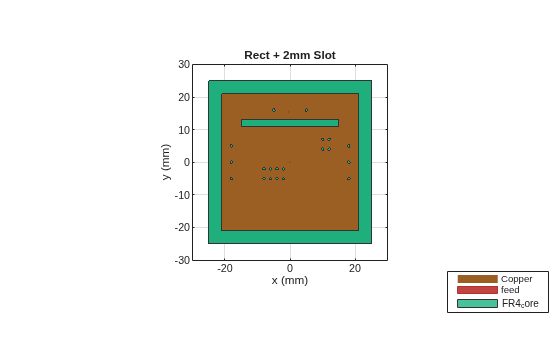
Rectangular + 2 mm routing slot — a 30 mm long, 2 mm wide channel for signal routing at y = +12 mm. Includes anti-pads.
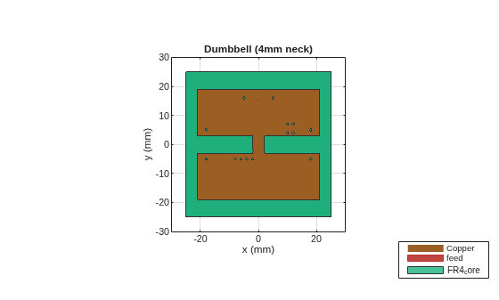
Dumbbell (4 mm neck) — two sub-cavities connected by a narrow bridge. Models a power plane serving two functional blocks.
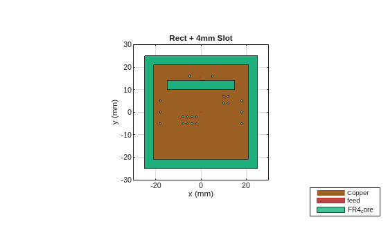
Rectangular + 4 mm routing slot — the layout team's request to widen the channel for additional DDR signal escape routes.
% Helper function to punch anti-pads into a plane shape
    function planeOut = punchAntipads(planeIn, viaXY, radius)
        planeOut = planeIn;
        for k = 1:size(viaXY,1)
            ap = antenna.Circle("Center",viaXY(k,:), "Radius",radius);
            planeOut = planeOut - ap;
        end
    end

% Variant 1: Solid reference
solidPlane = pwrBase;

% Variant 2: Rectangular + 2 mm routing slot
routingSlot = antenna.Rectangle("Center",[0,12*mm], ...
    "Length",30*mm, "Width",2*mm);
rectSlotPlane = punchAntipads(pwrBase - routingSlot, signalViaXY, antipadR);

% Variant 3: Dumbbell (4 mm neck)
topRect = antenna.Rectangle("Center",[0, 11*mm], "Length",42*mm, "Width",16*mm);
botRect = antenna.Rectangle("Center",[0,-11*mm], "Length",42*mm, "Width",16*mm);
neck    = antenna.Rectangle("Center",[0, 0],     "Length",4*mm,  "Width",6*mm);
dumbbellPlane = punchAntipads(topRect + botRect + neck, signalViaXY, antipadR);

% Variant 4: Rectangular + 4 mm routing slot (widened)
wideSlot = antenna.Rectangle("Center",[0,12*mm], "Length",30*mm, "Width",4*mm);
wideSlotPlane = punchAntipads(pwrBase - wideSlot, signalViaXY, antipadR);
Visualize Plane Geometries
Display each variant to verify geometry before running the solver. Anti-pads appear as small circular cutouts. The routing slot and dumbbell neck are the primary constrictions that force current to concentrate.
planeShapes = {solidPlane, rectSlotPlane, dumbbellPlane, wideSlotPlane};
planeNames  = ["Solid (reference)", "Rect + 2mm Slot", ...
    "Dumbbell (4mm neck)", "Rect + 4mm Slot"];
nVariants = numel(planeShapes);

for n = 1:nVariants
    figure;
    pShow = pcbComponent;
    pShow.BoardThickness = dielThick;
    pShow.BoardShape = traceRectangular("Length",boardL,"Width",boardW);
    pShow.Layers = {planeShapes{n}, sub, gnd};
    pShow.Conductor = metal('Copper');
    pShow.FeedDiameter = viaDia;
    pShow.FeedViaModel = 'hexagon';
    pShow.FeedLocations = [srcXY(1,:),1,3; senseXY,1,3];
    show(pShow); view(0,90);
    title(planeNames(n));
end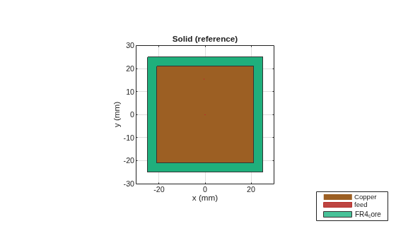
Run DC Analysis: Baseline Geometry
Demonstrate the full DC PI workflow on the rectangular + 2 mm slot geometry before running the comparative study.
The workflow is:
Build a
pcbComponentwith the desired plane shape, stackup, and via locationsCreate a
powerDistributionNetworkand assign source/load/sense portsSet DC operating conditions (nominal voltage, per-pin load current)
Call
voltage()andcurrent()to extract field solutions
pDC = pcbComponent;
pDC.BoardThickness = dielThick;
pDC.BoardShape = traceRectangular("Length",boardL,"Width",boardW);
pDC.Layers = {rectSlotPlane, sub, gnd};
pDC.Conductor = metal('Copper');
pDC.FeedDiameter = viaDia;
pDC.FeedViaModel = 'hexagon';
pDC.FeedLocations = [
    srcXY,   ones(nSrc,1),  3*ones(nSrc,1);
    loadXY,  ones(nLoad,1), 3*ones(nLoad,1);
    senseXY, 1, 3
];

pdn = powerDistributionNetwork(pDC);
setNetworkParameters(pdn, ...
    Source=sourceIdx, Load=loadIdx, Sense=senseIdx, ...
    PlatingThickness=25*mil);
  powerDistributionNetwork with properties:

   Network Parameters:
              NetType: [1×1 pcbComponent]
               Source: ["Vsource1"    "Vsource2"    "Vsource3"    "Vsource4"]
                 Load: ["Vload1"    "Vload2"    "Vload3"    "Vload4"    "Vload5"    "Vload6"    "Vload7"    "Vload8"]
                Sense: "Vsense1"
     PlatingThickness: 6.3500e-04

   DC Parameters:
       NominalVoltage: []
          LoadCurrent: []

   DC Rules:
    MaxCurrentDensity: []
           MinVoltage: []
           MaxVoltage: []
        MaxViaCurrent: []

   Port Parameters:
            NumPoints: 12
           CropRadius: 0

To Analyse PDN:
Set DC Parameters: setDCParameters
Set DC Rules: setDCRules
Set Port Parameters: setPortParameters
setDCParameters(pdn, ...
    "NominalVoltage", Vnom, ...
    "LoadCurrent", Iper*ones(1,nLoad));
  powerDistributionNetwork with properties:

   Network Parameters:
              NetType: [1×1 pcbComponent]
               Source: ["Vsource1"    "Vsource2"    "Vsource3"    "Vsource4"]
                 Load: ["Vload1"    "Vload2"    "Vload3"    "Vload4"    "Vload5"    "Vload6"    "Vload7"    "Vload8"]
                Sense: "Vsense1"
     PlatingThickness: 6.3500e-04

   DC Parameters:
       NominalVoltage: 0.8000
          LoadCurrent: [6.2500 6.2500 6.2500 6.2500 6.2500 6.2500 6.2500 6.2500]

   DC Rules:
    MaxCurrentDensity: []
           MinVoltage: []
           MaxVoltage: []
        MaxViaCurrent: []

   Port Parameters:
            NumPoints: 12
           CropRadius: 0

To Analyse PDN:
Set DC Rules: setDCRules
Set Port Parameters: setPortParameters
setDCRules(pdn, ...
    "MaxCurrentDensity", 2.0, ...
    "MaxVoltage", Vnom+0.05, "MinVoltage", Vnom-0.05, ...
    "MaxViaCurrent", 3.0);
  powerDistributionNetwork with properties:

   Network Parameters:
              NetType: [1×1 pcbComponent]
               Source: ["Vsource1"    "Vsource2"    "Vsource3"    "Vsource4"]
                 Load: ["Vload1"    "Vload2"    "Vload3"    "Vload4"    "Vload5"    "Vload6"    "Vload7"    "Vload8"]
                Sense: "Vsense1"
     PlatingThickness: 6.3500e-04

   DC Parameters:
       NominalVoltage: 0.8000
          LoadCurrent: [6.2500 6.2500 6.2500 6.2500 6.2500 6.2500 6.2500 6.2500]

   DC Rules:
    MaxCurrentDensity: 2
           MinVoltage: 0.7500
           MaxVoltage: 0.8500
        MaxViaCurrent: 3

   Port Parameters:
            NumPoints: 12
           CropRadius: 0


Set Port Parameters: setPortParameters
Visualize DC Voltage Distribution
The built-in voltage plot shows voltage deviation (mV) across the plane. Source vias (VRM region, top) are at high potential; load vias (ASIC region, center) are at lower potential. The gradient between them represents the IR drop consumed by plane resistance and current crowding at the routing slot.
figure;
voltage(pdn);
title("DC Voltage Deviation — Rect + 2mm Slot, 50 A");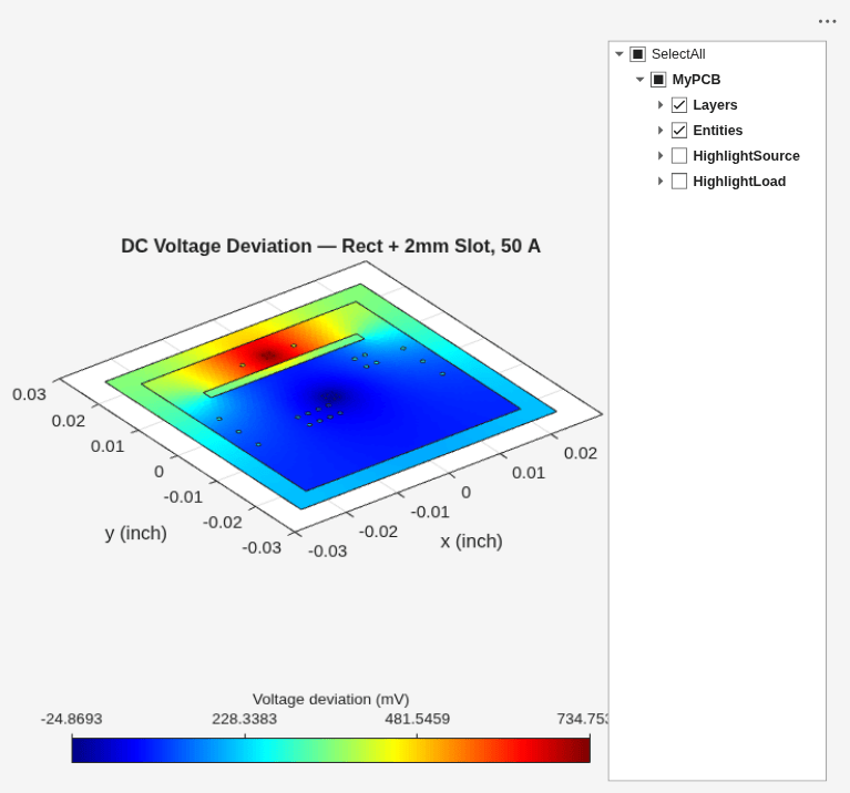
drawnow
Visualize DC Current Density
The current plot shows surface current density (A/m) on the power plane. Hot spots appear at:
Slot edges — the 2 mm constriction forces all current through a narrow bottleneck
Source via cluster — 50 A enters through only 4 vias
Dense anti-pad regions — current must navigate between clearance holes
figure;
current(pdn);
title("DC Current Density — Rect + 2mm Slot, 50 A");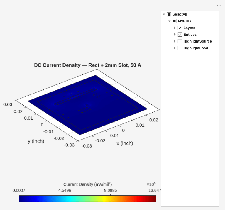
drawnow
Extract Numerical Results
The current function returns surface current density vectors (A/m) and mesh triangle centroids. The voltage function returns voltage deviation (mV) at mesh nodes. These outputs enable quantitative comparison across geometry variants.
[Jvec, xyCentroids] = current(pdn);
Jmag = vecnorm(Jvec, 2, 2);

[Vout, xyV] = voltage(pdn);
Peak surface current density and volumetric current density (dividing by copper thickness):
peakJs_Am = max(Jmag)
peakJs_Am =
4.8530e+04
peakJ_Amm2 = max(Jmag) / (cuThick * 1e6)
peakJ_Amm2 =
1.3866e+03
IR drop from source to sense point:
% Find voltage at sense point (nearest mesh node to origin)
dSense = sqrt(xyV(:,1).^2 + xyV(:,2).^2);
[~, idxSense] = min(dSense);
V_sense_mV = Vout(idxSense);

% Find max source via voltage
V_src_mV = zeros(nSrc, 1);
for k = 1:nSrc
    dV = sqrt((xyV(:,1)-srcXY(k,1)).^2 + (xyV(:,2)-srcXY(k,2)).^2);
    [~, idx] = min(dV);
    V_src_mV(k) = Vout(idx);
end
IR_drop_mV = max(V_src_mV) - V_sense_mV
IR_drop_mV =
700.9961
Comparative DC Analysis: All Variants
Run the full DC analysis for each geometry variant and collect key metrics. The solid reference (no cutouts) establishes the theoretical floor for IR drop and current density. Any increase above this floor is the cost of geometric discontinuities in the power plane.
results = struct();

for n = 1:nVariants
    pDCn = pcbComponent;
    pDCn.BoardThickness = dielThick;
    pDCn.BoardShape = traceRectangular("Length",boardL,"Width",boardW);
    pDCn.Layers = {planeShapes{n}, sub, gnd};
    pDCn.Conductor = metal('Copper');
    pDCn.FeedDiameter = viaDia;
    pDCn.FeedViaModel = 'hexagon';
    pDCn.FeedLocations = [
        srcXY,   ones(nSrc,1),  3*ones(nSrc,1);
        loadXY,  ones(nLoad,1), 3*ones(nLoad,1);
        senseXY, 1, 3
    ];

    pdnN = powerDistributionNetwork(pDCn);
    setNetworkParameters(pdnN, ...
        Source=sourceIdx, Load=loadIdx, Sense=senseIdx, ...
        PlatingThickness=25*mil);
    setDCParameters(pdnN, ...
        "NominalVoltage", Vnom, ...
        "LoadCurrent", Iper*ones(1,nLoad));
    setDCRules(pdnN, ...
        "MaxCurrentDensity", 2.0, ...
        "MaxVoltage", Vnom+0.05, "MinVoltage", Vnom-0.05, ...
        "MaxViaCurrent", 3.0);

    % Extract current density
    [Jn, xyN] = current(pdnN);
    JmagN = vecnorm(Jn, 2, 2);

    % Extract voltage
    [Vn, xyVn] = voltage(pdnN);

    % Voltage at sense point
    dS = sqrt(xyVn(:,1).^2 + xyVn(:,2).^2);
    [~, iS] = min(dS);

    % Max source via voltage
    Vsrc = zeros(nSrc,1);
    for k = 1:nSrc
        dV = sqrt((xyVn(:,1)-srcXY(k,1)).^2 + (xyVn(:,2)-srcXY(k,2)).^2);
        [~, idx] = min(dV);
        Vsrc(k) = Vn(idx);
    end

    results(n).name = planeNames(n);
    results(n).peakJ_Am = max(JmagN);
    results(n).peakJ_Amm2 = max(JmagN) / (cuThick * 1e6);
    results(n).V_sense_mV = Vn(iS);
    results(n).IR_drop_mV = max(Vsrc) - Vn(iS);
    results(n).Jdata = JmagN;
    results(n).xyJ = xyN;
end
  powerDistributionNetwork with properties:

   Network Parameters:
              NetType: [1×1 pcbComponent]
               Source: ["Vsource1"    "Vsource2"    "Vsource3"    "Vsource4"]
                 Load: ["Vload1"    "Vload2"    "Vload3"    "Vload4"    "Vload5"    "Vload6"    "Vload7"    "Vload8"]
                Sense: "Vsense1"
     PlatingThickness: 6.3500e-04

   DC Parameters:
       NominalVoltage: []
          LoadCurrent: []

   DC Rules:
    MaxCurrentDensity: []
           MinVoltage: []
           MaxVoltage: []
        MaxViaCurrent: []

   Port Parameters:
            NumPoints: 12
           CropRadius: 0

To Analyse PDN:
Set DC Parameters: setDCParameters
Set DC Rules: setDCRules
Set Port Parameters: setPortParameters
  powerDistributionNetwork with properties:

   Network Parameters:
              NetType: [1×1 pcbComponent]
               Source: ["Vsource1"    "Vsource2"    "Vsource3"    "Vsource4"]
                 Load: ["Vload1"    "Vload2"    "Vload3"    "Vload4"    "Vload5"    "Vload6"    "Vload7"    "Vload8"]
                Sense: "Vsense1"
     PlatingThickness: 6.3500e-04

   DC Parameters:
       NominalVoltage: 0.8000
          LoadCurrent: [6.2500 6.2500 6.2500 6.2500 6.2500 6.2500 6.2500 6.2500]

   DC Rules:
    MaxCurrentDensity: []
           MinVoltage: []
           MaxVoltage: []
        MaxViaCurrent: []

   Port Parameters:
            NumPoints: 12
           CropRadius: 0

To Analyse PDN:
Set DC Rules: setDCRules
Set Port Parameters: setPortParameters
  powerDistributionNetwork with properties:

   Network Parameters:
              NetType: [1×1 pcbComponent]
               Source: ["Vsource1"    "Vsource2"    "Vsource3"    "Vsource4"]
                 Load: ["Vload1"    "Vload2"    "Vload3"    "Vload4"    "Vload5"    "Vload6"    "Vload7"    "Vload8"]
                Sense: "Vsense1"
     PlatingThickness: 6.3500e-04

   DC Parameters:
       NominalVoltage: 0.8000
          LoadCurrent: [6.2500 6.2500 6.2500 6.2500 6.2500 6.2500 6.2500 6.2500]

   DC Rules:
    MaxCurrentDensity: 2
           MinVoltage: 0.7500
           MaxVoltage: 0.8500
        MaxViaCurrent: 3

   Port Parameters:
            NumPoints: 12
           CropRadius: 0


Set Port Parameters: setPortParameters
  powerDistributionNetwork with properties:

   Network Parameters:
              NetType: [1×1 pcbComponent]
               Source: ["Vsource1"    "Vsource2"    "Vsource3"    "Vsource4"]
                 Load: ["Vload1"    "Vload2"    "Vload3"    "Vload4"    "Vload5"    "Vload6"    "Vload7"    "Vload8"]
                Sense: "Vsense1"
     PlatingThickness: 6.3500e-04

   DC Parameters:
       NominalVoltage: []
          LoadCurrent: []

   DC Rules:
    MaxCurrentDensity: []
           MinVoltage: []
           MaxVoltage: []
        MaxViaCurrent: []

   Port Parameters:
            NumPoints: 12
           CropRadius: 0

To Analyse PDN:
Set DC Parameters: setDCParameters
Set DC Rules: setDCRules
Set Port Parameters: setPortParameters
  powerDistributionNetwork with properties:

   Network Parameters:
              NetType: [1×1 pcbComponent]
               Source: ["Vsource1"    "Vsource2"    "Vsource3"    "Vsource4"]
                 Load: ["Vload1"    "Vload2"    "Vload3"    "Vload4"    "Vload5"    "Vload6"    "Vload7"    "Vload8"]
                Sense: "Vsense1"
     PlatingThickness: 6.3500e-04

   DC Parameters:
       NominalVoltage: 0.8000
          LoadCurrent: [6.2500 6.2500 6.2500 6.2500 6.2500 6.2500 6.2500 6.2500]

   DC Rules:
    MaxCurrentDensity: []
           MinVoltage: []
           MaxVoltage: []
        MaxViaCurrent: []

   Port Parameters:
            NumPoints: 12
           CropRadius: 0

To Analyse PDN:
Set DC Rules: setDCRules
Set Port Parameters: setPortParameters
  powerDistributionNetwork with properties:

   Network Parameters:
              NetType: [1×1 pcbComponent]
               Source: ["Vsource1"    "Vsource2"    "Vsource3"    "Vsource4"]
                 Load: ["Vload1"    "Vload2"    "Vload3"    "Vload4"    "Vload5"    "Vload6"    "Vload7"    "Vload8"]
                Sense: "Vsense1"
     PlatingThickness: 6.3500e-04

   DC Parameters:
       NominalVoltage: 0.8000
          LoadCurrent: [6.2500 6.2500 6.2500 6.2500 6.2500 6.2500 6.2500 6.2500]

   DC Rules:
    MaxCurrentDensity: 2
           MinVoltage: 0.7500
           MaxVoltage: 0.8500
        MaxViaCurrent: 3

   Port Parameters:
            NumPoints: 12
           CropRadius: 0


Set Port Parameters: setPortParameters
  powerDistributionNetwork with properties:

   Network Parameters:
              NetType: [1×1 pcbComponent]
               Source: ["Vsource1"    "Vsource2"    "Vsource3"    "Vsource4"]
                 Load: ["Vload1"    "Vload2"    "Vload3"    "Vload4"    "Vload5"    "Vload6"    "Vload7"    "Vload8"]
                Sense: "Vsense1"
     PlatingThickness: 6.3500e-04

   DC Parameters:
       NominalVoltage: []
          LoadCurrent: []

   DC Rules:
    MaxCurrentDensity: []
           MinVoltage: []
           MaxVoltage: []
        MaxViaCurrent: []

   Port Parameters:
            NumPoints: 12
           CropRadius: 0

To Analyse PDN:
Set DC Parameters: setDCParameters
Set DC Rules: setDCRules
Set Port Parameters: setPortParameters
  powerDistributionNetwork with properties:

   Network Parameters:
              NetType: [1×1 pcbComponent]
               Source: ["Vsource1"    "Vsource2"    "Vsource3"    "Vsource4"]
                 Load: ["Vload1"    "Vload2"    "Vload3"    "Vload4"    "Vload5"    "Vload6"    "Vload7"    "Vload8"]
                Sense: "Vsense1"
     PlatingThickness: 6.3500e-04

   DC Parameters:
       NominalVoltage: 0.8000
          LoadCurrent: [6.2500 6.2500 6.2500 6.2500 6.2500 6.2500 6.2500 6.2500]

   DC Rules:
    MaxCurrentDensity: []
           MinVoltage: []
           MaxVoltage: []
        MaxViaCurrent: []

   Port Parameters:
            NumPoints: 12
           CropRadius: 0

To Analyse PDN:
Set DC Rules: setDCRules
Set Port Parameters: setPortParameters
  powerDistributionNetwork with properties:

   Network Parameters:
              NetType: [1×1 pcbComponent]
               Source: ["Vsource1"    "Vsource2"    "Vsource3"    "Vsource4"]
                 Load: ["Vload1"    "Vload2"    "Vload3"    "Vload4"    "Vload5"    "Vload6"    "Vload7"    "Vload8"]
                Sense: "Vsense1"
     PlatingThickness: 6.3500e-04

   DC Parameters:
       NominalVoltage: 0.8000
          LoadCurrent: [6.2500 6.2500 6.2500 6.2500 6.2500 6.2500 6.2500 6.2500]

   DC Rules:
    MaxCurrentDensity: 2
           MinVoltage: 0.7500
           MaxVoltage: 0.8500
        MaxViaCurrent: 3

   Port Parameters:
            NumPoints: 12
           CropRadius: 0


Set Port Parameters: setPortParameters
  powerDistributionNetwork with properties:

   Network Parameters:
              NetType: [1×1 pcbComponent]
               Source: ["Vsource1"    "Vsource2"    "Vsource3"    "Vsource4"]
                 Load: ["Vload1"    "Vload2"    "Vload3"    "Vload4"    "Vload5"    "Vload6"    "Vload7"    "Vload8"]
                Sense: "Vsense1"
     PlatingThickness: 6.3500e-04

   DC Parameters:
       NominalVoltage: []
          LoadCurrent: []

   DC Rules:
    MaxCurrentDensity: []
           MinVoltage: []
           MaxVoltage: []
        MaxViaCurrent: []

   Port Parameters:
            NumPoints: 12
           CropRadius: 0

To Analyse PDN:
Set DC Parameters: setDCParameters
Set DC Rules: setDCRules
Set Port Parameters: setPortParameters
  powerDistributionNetwork with properties:

   Network Parameters:
              NetType: [1×1 pcbComponent]
               Source: ["Vsource1"    "Vsource2"    "Vsource3"    "Vsource4"]
                 Load: ["Vload1"    "Vload2"    "Vload3"    "Vload4"    "Vload5"    "Vload6"    "Vload7"    "Vload8"]
                Sense: "Vsense1"
     PlatingThickness: 6.3500e-04

   DC Parameters:
       NominalVoltage: 0.8000
          LoadCurrent: [6.2500 6.2500 6.2500 6.2500 6.2500 6.2500 6.2500 6.2500]

   DC Rules:
    MaxCurrentDensity: []
           MinVoltage: []
           MaxVoltage: []
        MaxViaCurrent: []

   Port Parameters:
            NumPoints: 12
           CropRadius: 0

To Analyse PDN:
Set DC Rules: setDCRules
Set Port Parameters: setPortParameters
  powerDistributionNetwork with properties:

   Network Parameters:
              NetType: [1×1 pcbComponent]
               Source: ["Vsource1"    "Vsource2"    "Vsource3"    "Vsource4"]
                 Load: ["Vload1"    "Vload2"    "Vload3"    "Vload4"    "Vload5"    "Vload6"    "Vload7"    "Vload8"]
                Sense: "Vsense1"
     PlatingThickness: 6.3500e-04

   DC Parameters:
       NominalVoltage: 0.8000
          LoadCurrent: [6.2500 6.2500 6.2500 6.2500 6.2500 6.2500 6.2500 6.2500]

   DC Rules:
    MaxCurrentDensity: 2
           MinVoltage: 0.7500
           MaxVoltage: 0.8500
        MaxViaCurrent: 3

   Port Parameters:
            NumPoints: 12
           CropRadius: 0


Set Port Parameters: setPortParameters
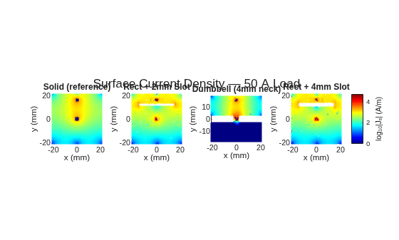
Current Density Comparison (Log Scale)
Log-scale scatter plots reveal how each geometry forces current through constrictions. The solid reference shows smooth, low-magnitude current distribution. The dumbbell neck and slot edges produce intense local concentration.
figure;
tiledlayout(1,nVariants,'TileSpacing','compact');
allJvals = vertcat(results.Jdata);
cMin = log10(max(min(allJvals(allJvals>0)), 1));
cMax = log10(max(allJvals));

for n = 1:nVariants
    nexttile;
    Jlog = log10(max(results(n).Jdata, 10^cMin));
    scatter(results(n).xyJ(:,1)*1e3, results(n).xyJ(:,2)*1e3, ...
        3, Jlog, 'filled');
    colormap(gca, jet);
    clim([cMin cMax]);
    axis equal tight;
    title(results(n).name,'FontSize',9);
    xlabel("x (mm)"); ylabel("y (mm)");
end
cb = colorbar; cb.Label.String = "log_{10}|J_s| (A/m)";
sgtitle("Surface Current Density — " + Itotal + " A Load");
DC Metrics Summary
This table is the primary deliverable from a DC PI analysis. It reports:
IR Drop (mV) — total voltage loss from VRM to ASIC sense point (includes via barrel and plane spreading resistance)
Delta IR (mV) — incremental IR drop relative to the solid reference, isolating the cost of geometric features
Peak J (A/mm²) — maximum volumetric current density (), for comparison against IPC-2152 limits
Src Via (A) and Load Via (A) — per-via current (equal-split assumption for sources; fixed boundary condition for loads)
Geometry = planeNames(:);
V_sense_mV = [results.V_sense_mV]';
IR_Drop_mV = [results.IR_drop_mV]';
Delta_IR_mV = IR_Drop_mV - IR_Drop_mV(1);
Peak_Js_Am = [results.peakJ_Am]';
Peak_J_Amm2 = [results.peakJ_Amm2]';
Src_Via_A = repmat(Itotal/nSrc, nVariants, 1);
Load_Via_A = repmat(Iper, nVariants, 1);

dcMetrics = table(Geometry, IR_Drop_mV, Delta_IR_mV, Peak_Js_Am, Peak_J_Amm2, Src_Via_A, Load_Via_A)
dcMetrics = 4×7 table
          Geometry           IR_Drop_mV    Delta_IR_mV    Peak_Js_Am    Peak_J_Amm2    Src_Via_A    Load_Via_A
    _____________________    __________    ___________    __________    ___________    _________    __________

    "Solid (reference)"        489.75             0         31982         913.78         12.5          6.25
    "Rect + 2mm Slot"             701        211.25         48530         1386.6         12.5          6.25
    "Dumbbell (4mm neck)"      645.42        155.68         42872         1224.9         12.5          6.25
    "Rect + 4mm Slot"          717.71        227.96         51057         1458.8         12.5          6.25
Interpreting the Results
Delta IR isolates the cost of each geometric feature by subtracting the solid-reference baseline:
Anti-pads + 2 mm slot: adds significant resistance to the current path due to the bottleneck at the slot edges.
Dumbbell (4 mm neck): the narrow neck forces all 50 A through a 4 mm bridge, but because it is shorter than the slot, the total path resistance is lower than the full-width slot.
Widened 4 mm slot: removing more copper from the current path increases both IR drop and peak J. The layout team's request to widen the routing channel has a quantifiable DC cost.
Peak J provides a via current limit check per IPC-2152. However, peak J alone does not predict thermal behavior — a narrow hotspot in J spreads heat quickly into surrounding copper, while a broad region of elevated J accumulates more total heat. For thermal risk assessment, combine this DC analysis with steady-state thermal modeling (see companion example PDN_DC_Thermal_Exploration).
Effect of Load Current on IR Drop
DC PI analysis is linear: IR drop scales proportionally with current. This makes it straightforward to evaluate a design across the full operating range without re-running the solver. Demonstrate by scaling from the baseline result.
I_sweep = [20 35 50 65 80]';
scaleFactor = I_sweep / Itotal;

% Scale from baseline (variant 2) results
baselineIR = results(2).IR_drop_mV;
IR_scaled = baselineIR * scaleFactor;

figure;
bar(I_sweep, IR_scaled);
xlabel("Total Load Current (A)");
ylabel("IR Drop (mV)");
title("IR Drop vs. Load Current — Rect + 2mm Slot");
grid on;
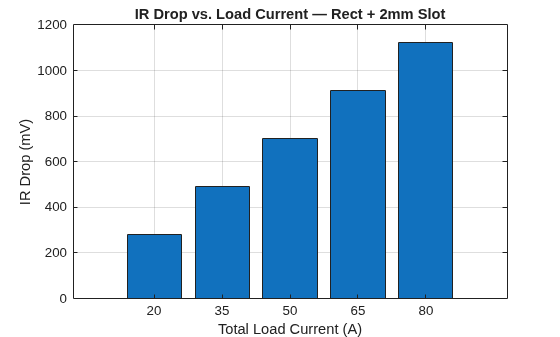
The linear relationship confirms that a single DC solve at rated current is sufficient to characterize the full operating range. At 80 A (a typical next-generation AI accelerator), the IR drop is 60% higher than at 50 A — this may consume critical voltage margin and motivate geometry changes.
IR_vs_Current = table(I_sweep, IR_scaled, ...
    'VariableNames', ["Load_A", "IR_Drop_mV"])
IR_vs_Current = 5×2 table
    Load_A    IR_Drop_mV
    ______    __________

      20         280.4
      35         490.7
      50           701
      65        911.29
      80        1121.6
Design Guidelines from DC PI Analysis
Based on the comparative results, a PI engineer can provide these quantitative recommendations to the layout team:
Routing slot width matters nonlinearly. Widening from 2 mm to 4 mm increases IR drop, but the dumbbell (which has a more severe constriction) may have lower total IR drop because its bottleneck is shorter. Path length and constriction width both contribute.
Anti-pads are a hidden cost. The Delta IR between the solid reference and the slotted plane includes contributions from both the routing slot and the 20 signal via anti-pads. A swiss-cheese via field under the BGA degrades DC performance even without routing channels.
Peak J identifies reliability risk. Current density exceeding IPC-2152 limits at operating temperature indicates potential long-term copper fatigue. Flag any region where A/mm² for design review.
Source via count is a first-order lever. Each additional source via in parallel reduces the per-via current and the local current density at the VRM connection point. For high-current rails (>50 A), use at least 4 source vias.
Summary
This example demonstrated the complete DC PI analysis workflow using RF PCB Toolbox:
pcbComponentdefines arbitrary plane geometries using antenna shape primitives (rectangles, circles, Boolean subtraction)powerDistributionNetworkconfigures the DC operating point and extracts voltage and current densityA solid reference plane validates the solver and establishes the IR drop floor
MATLAB table objects present metrics suitable for design review documentation
The DC analysis runs in seconds per variant, making it practical to evaluate dozens of geometry options during the pre-layout phase — long before committing to a PCB layout tool.

