Analyze Backplane with Line Cards
This example shows how to analyze a serial link consisting of a backplane and two line cards with the Serial Link Designer app. You can model the SerDes drivers/receivers, capture a topology for analysis, run network characterization, and evaluate the impact of different solution space variables on your design's performance.
The serial link to be modeled is a backplane with two line cards.
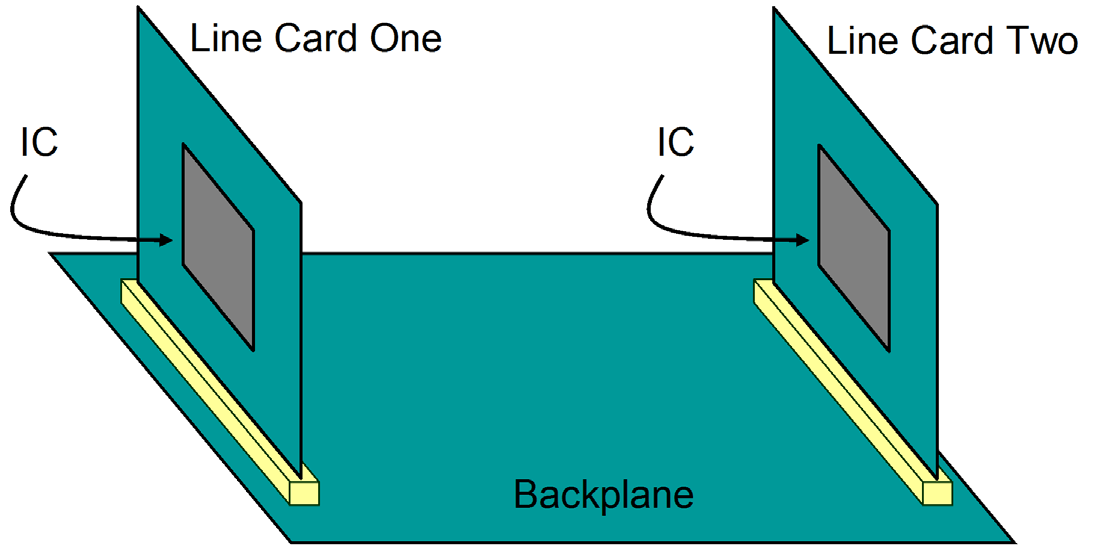
The channel topology is represented by:
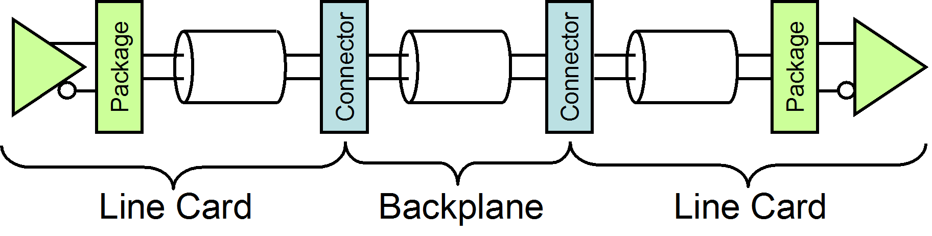
The packages and connectors are modeled with S-Parameters. The traces are modeled with w-lines.
Create New Project
Open the Serial Link Designer app.
serialLinkDesigner
Create a new project by selecting File > Project > New Project. In the newly opened dialog box, name the project as backplane_linecard, the interface as serdes, and the schematic sheet as channel. The Pre-Layout Analysis tab shows the blank schematic sheet.

Setup Libraries
You can create the library elements for the transmission lines, packages, connectors, and designators.
Create a differential lossy transmission line model based on a stripline cross-section. Select Tools > Lossy Transmission Line Editor. In the newly opened Lossy Transmission Line Editor dialog box, select Differential and select Model Type as Stripline.
The traces are 4 mils wide and 0.65 mils thick. They are 9.0 mils above and 8.5 mils below planes with a dielectric constant of Er 4.25. The trace separation is 5 mils. So change the parameters Dielectric Height (H1 in mils) to 9, Dielectric Height (H2 in mils) to 8.5, and Differential Separation (mils) to 5.
Click the Calculate button to run the 2-D field solver. The Impedance at the bottom left changes from derived to the calculated value.
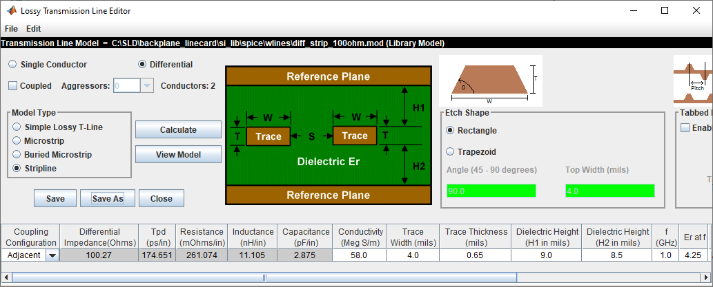
Click the Save As button to save the model in the project’s library. Use the default name diff_strip_100ohm. Make sure the directory is <Project Library>/spice/wlines. Close the Lossy Transmission Line Editor.
Four custom S-Parameter data files (connector_ab.s4p, connector_cd.s4p, connector_ef.s4p, and connector_gh.s4p) are attached as supporting files to this example. Download all four Touchstone® (.s4p) files. To import the connector S-Parameter data, select Libraries > Import S-Parameter. Browse to the location where you saved the downloaded Touchstone files and select all four. Verify that the Merge Wrappers checkbox is selected on the Import S-Parameter File(s) dialog box. Merging the connector wrappers makes it possible to sweep them. Import the files. This launches the Edit S-Parameter Port Maps dialog box. The dialog box contains a separate tab for each connector file.

The table on the left shows the loss at 50 MHz between each pair of ports. The cells in white show the smallest loss. Generally, the smallest loss occurs at the ports that are the through path. The blue cells indicate the left-hand differential port. The green cells indicate the right-hand differential port.
The table on the right shows orientation of the S-parameter block as it will be on the schematic sheet and identifies the differential ports.
To view the through path dB vs. frequency responses of the single-ended paths, click the Display Waveforms button. This launches the Signal Integrity Viewer app.

You can add new display to view all the data in real/imaginary, magnitude/angle and dB. Close the Signal Integrity Viewer app, Edit S-Parameter Port Maps dialog box, and Import S-Parameter File(s) dialog box.
Create Channel Schematic
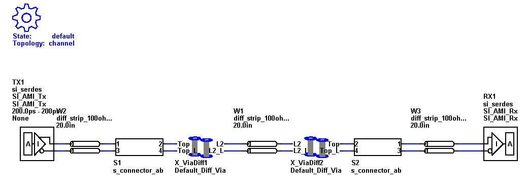
Add the backplane transmission line by selecting the differential lossy transmission line element to the blank canvas on the Pre-Layout Analysis tab. Right-click on the symbol and choose Select T-Line Model. Switch to the <Project Library>/spice/wlines library if it is not selected. Select the diff_strip_100ohm model.
Add two differential via models between the backplane traces and the connector.
To start, add a new differential via element with 12 layers of connecting layers to create the default stackup to the left of the transmission line. Right-click on the via symbol and choose Edit Differential Via Model to launch the Via Editor dialog box. The default via connects the top layer to the bottom layer. Uncheck the Left Via Connect and Right Via Connect checkboxes for the layer Bottom and check the checkboxes for layer L2. This changes the via to a via that is connecting the layer Top to the layer L2. It is still a through-hole via with a stub from layer L2 to the bottom of the board. To model a backdrilled via check Enable in the Backdrill panel, check By Layer, then select layer P2 in the list for Bottom. The layers view will change to show that the barrel of the via is gone from the bottom through layer P2.

Save and close the Via Editor dialog box. Copy, paste, and mirror another via to the right of the transmission line.
To add the connectors, add a new S-Parameter element. Choose connector_s4p.smod and s_connector_ab from the <Project Library>/spice/s_params directory in the Select S-Parameter Model dialog box. Add two connectors (mirrored) on the left and right of the vias.
Copy the backplane transmission line symbol and paste one copy on the far left and one copy on the far right to represent the traces on the two line cards. Add two differential buffer elements (mirrored) and place one in the far left to designate the transmitter and one in the far right to designate the receiver.
Connect the elements together to complete the schematic.
Double-click on one of the W-line symbols to launch the Lossy Transmission Line Element Properties dialog box. Enable the Sweep Length checkbox for each w-line. Change the name of the backplane symbol to $bp_len and the line card symbols to $lc_len. By changing the two line card w-lines to the same name you can use the same solution space variable for both w-line symbols. Close the Lossy Transmission Line Element Properties dialog box.
In the Solution Space panel, change the Value 1 value for Variable $bp_len to 16in and Variable $lc_len to 3in.
Double-click on one of the connector symbols to launch the Spice Subcircuit Element Properties dialog box. There are two rows, one for each connector symbol. Enable the Sweep Model checkbox in each row and change the variable names to $connector.
Double click on the TX symbol to launch the Designator Element Properties dialog box. Set the UI (Unit Interval) for TX1 to Serdes_10G by selecting it from the dropdown menu of the UI parameter. The UI is set to 100 ps. Save the changes to the schematic.
Validate the schematic set by selecting Run > Validate Current Schematic Set. The validation should run without warning or errors.
Network Characterization
To see the effects of sweeping the package model, connector model, and line card trace lengths on the physical channel characteristics, run network characterization. Network characterization derives the LTI signature of the analog network. The analog network includes the analog TX and RX characteristics as well as the channel elements themselves. The Serial Link Designer app frequency domain network solver derives the transfer function of the analog network. From the transfer function, the app derives the impulse and step response. The app also derives the pulse response using the UI set during schematic creation. It also computes the insertion loss, return loss, ripple, impulse width and other metrics.
To sweep the connector model, select the $connector Variable, right click and select Set All Values. The solution space becomes populated with the four models you imported.
To sweep the line card length, select the $lc_len Variable and add the values 2in, 4in, and 5in. Save the changes.

Run the simulation by selecting Run > Simulate Selected. In the Prelayout Channel Analysis dialog box, select Validate, Generate Netlists, Perform Channel Analysis, and Autoload Results. Make sure Include Statistical Analysis and Include Time Domain Analysis are unchecked, so network characterization is the only analysis performed. Click Run to start the simulation process.
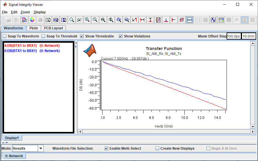
When the analysis is finished the Signal Integrity Viewer app launches and loads the analysis results. The table has one row per simulation. You can sort by any column by clicking on the column header. For this example, the difference between the lowest (16.67dB) and highest (21.54dB) loss is around 5 dB.

To view the transfer function of any data, select the data, right click and select Show Transfer Function (Unequalized).
Close the Signal Integrity Viewer app and the Prelayout Channel Analysis dialog box.
Statistical Channel Analysis
Statistical analysis can analyze the channel with LTI TX and RX equalization. This example shows how you can sweep the TX equalization and RX CTLE for statistical analysis.
To remove the solution space entries for the connector model, select the $connector Variable, right click and select Set to Default. This will leave an entry in Value 1 only for the connector. Delete the entries for 4in and 5in for $lc_len by removing the columns.
Select the symbol for TX1 on the schematic to highlight the solution space table rows for the TX AMI parameters. The transmitter has three taps in the Variation Group TX1:tap. Delete the variation group from the taps so that they can be swept independently.
Select the TX1:tap_filter.0 Variable and add the values 0.9, 0.8, and 0.7.
Select the TX1:tap_filter.1 Variable and add the values -0.2, -0.1, 0.1, and 0.2. Save the changes.

Run the simulation. In the Prelayout Channel Analysis dialog box, select Validate, Generate Netlists, Include Statistical Analysis, Perform Channel Analysis, and Autoload Results. The Signal Integrity Viewer app launches when the simulation is complete.
On the Statistical tab of the Signal Integrity Viewer window, click on the column header for Stat Eye Margin (V). The margin is negative on all of the simulation. In fact the eye is completely closed on all sims, so TX equalization is not enough to get this channel working.
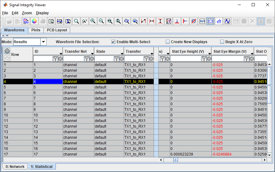

Click on the Stat BER header to get the smallest BER (4.64e-10 in this example) at the top. To see the tap settings for the top row right-click on the row in the table and select Show Solution Space. In the dialog that appears you can see the tap settings: TX1.tap_filter.0 = 0.7 and TX1.tap_filter.1 = -0.2.
Go back to the Serial Link Designer app Solution Space panel. Change the TX equalizer taps to the values that gave the best BER from above (0.0, 0.7, -0.2, 0.0). Change Value 2 for RX1:peaking_filter.mode to Auto.

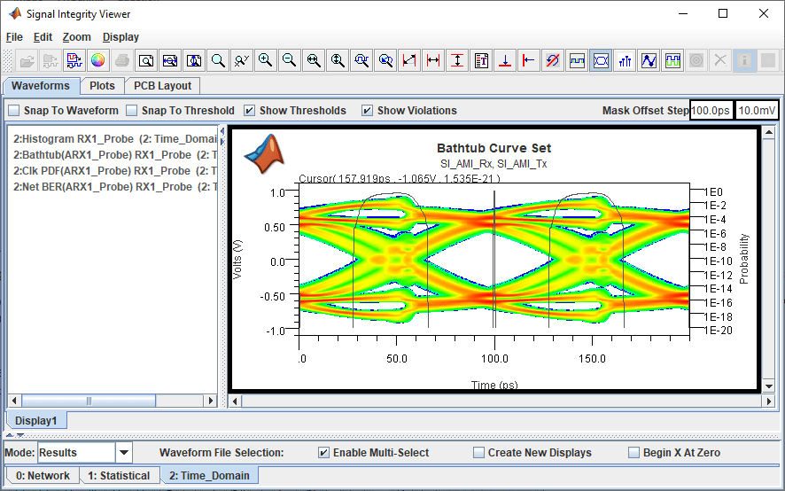
Save the changes and rerun the simulation. Two of the four simulations now show positive statistical eye margin. Select one of the rows with a positive margin, right click and select Show BER. You can see the statistical eye, the bathtub curve and the clock PDF.

Close the Signal Integrity Viewer app and the Prelayout Channel Analysis dialog box.
Time Domain Analysis
The DFE adaptation behavior is non-LTI, so running time domain analysis will let you see how the DFE converges over time.
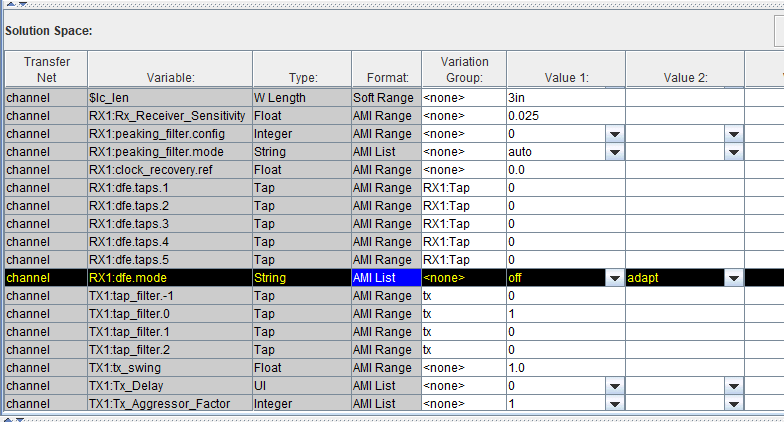
To set up the time domain analysis, in the Solution Space panel of the Serial Link Designer app, delete the Value 2 (2in) of the $lc_len Variable. Set the values of Variable RX1:peaking_filter.mode Value 1 to auto and Value 2 to blank. Change the Variation Group of TX1 tap filters to tx and set the values of (0, 1, 0, 0). Set the Value 2 to of RX1:dfe.mode Variable to adapt.
Select Setup > Simulation Parameters and check that the Time Domain Stop is set to 1,000,000 UI and the Record Bits is set to 2,500 UI. Right-click on the RX symbol on the schematic and select Edit AMI File(s). In the AMI file that opens the Ignore_Bits parameter is set to 500,000 UI. The largest value of either the AMI file parameter Ignore_Bits or the Simulation Parameters setting for Ignore_Bits is used during simulation. In this case, the value of 500,000 UI from the AMI file will be used instead of the value of 10,000 UI in Simulation Parameters. This group of settings configures the simulation to run for one million UI. The last 500,000 UI is used for the persistent eye and the BER and the last 2500 UI of the waveform is saved.

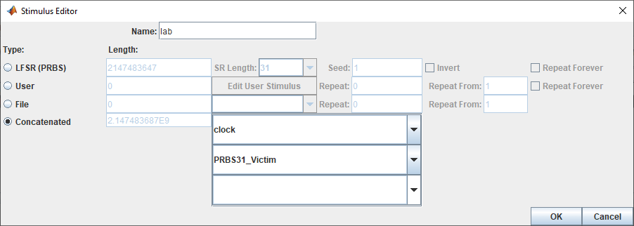
Double click on the TX symbol on the schematic to launch the Designator Element Properties dialog box. Click on the Stimulus button to open the Stimuli dialog box. Click on New button to create a new stimulus. Set the Name to lab and Type to Concatenated. Make it a concatenated stimulus that is clock followed by PRBS31_Victim. Save the changes.
On the Designator Element Properties dialog box, select the Stimulus as lab. Save the changes. Run the simulation and select Include Time Domain Analysis in the Prelayout Channel Analysis dialog box.
The Signal Integrity Viewer app launches when the simulation is complete. Select the Time_Domain tab and right click on the result rows and select Show Solution Space to see which row is showing the result of the DFE adapt mode. Select the row corresponding to the DFE adapt mode, right click and select Show BER.
Right click on the Display panel and add a new display. On the Time_Domain tab right-click on the results row for the DFE Adapt simulation and select Show IBIS-AMI Output Parameters > RX1_SiSoft_AMI_Rx. Delete the nodes that are not DFE taps and zoom to view the tap coefficients over time as they adapt.

Close the Signal Integrity Viewer app and the Prelayout Channel Analysis dialog box.