Model AXI Manager Interface
Various video processing applications require random pixel access into stored image data. For instance, some algorithms operate across one dimension of a video frame (lines), then compute further data across the other dimension of the frame (columns). The design must be able to access the stored image pixels in any order. Other uses of random pixel access include pixel overlay or image compression and decompression.
This support package provides a simulation model of an external memory interface that gives read and write access to any address. It also provides interfaces on the FPGA reference design that connect to external memory on the board. The reference design implements the memory interface using AXI manager.
Note
An external memory interface is not supported with multipixel streaming. You can use this interface with a MIPI® FMC card.
To model the external memory interface, start your design using one of the Pixel-Streaming Design with External Memory template models. See Create Model Using Simulink Templates. The template includes a subsystem that models the external memory interface. If you are using a MIPI FMC card, in the template model, replace the Video Capture HDMI block with the Video Capture MIPI block, and replace the blocks in the Conversion area with RGB Vector to Packed RGB and Packed RGB to RGB Vector blocks. You can copy these blocks from the Corner Detection with Zynq-Based Hardware and MIPI Sensor example.
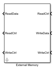
The External Memory subsystem provides a simplified model of the independent read and
write interfaces to the memory, modeled using HDL Coder™
Dual Port RAM blocks. The ReadCtrl and
WriteCtrl ports are buses that contain memory control signals.
The WriteData port expects uint32 or
uint64 type. The data type of ReadData
matches the data type of WriteData. The subsystem does not simulate
the physical memory bus protocol, timing, or contention. For details of this simplified
memory protocol, see Model Design for AXI4 Master Interface Generation (HDL Coder).

Alternatively, copy the External Memory subsystem found in the Image Rotation with Zynq-Based Hardware example. Connect this subsystem to your FPGA-targeted subsystem.
To increase efficiency, consider packing pixel data for writes into 32-bit or 64-bit words, and performing writes in consecutive bursts.
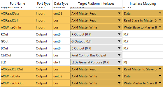
For deployment to FPGA, map the external memory interface ports of your FPGA user logic to the external memory interface in the reference design. At step 1.3 in HDL Workflow Advisor, select the AXI Master Read and AXI Master Write interfaces, as shown.

The reference design reserves a 64Mb address space for AXI manager use, and assigns a fixed address offset. The device tree of the board operating system ensures other processes cannot access the same memory space. Access the memory from your FPGA user logic by specifying the address offset from 0. The AXI manager interface logic translates your request to the actual address.