Astable Oscillator
This example shows an implementation of an astable oscillator circuit. The circuit output voltage V2 oscillates in an unstable fashion between high and low states.
At time zero both transistors are off and the voltages across C1 and C2 are zero. C1 starts to charge via R4 and Transistor 1 base-emitter junction. Similarly C2 charges via R2 and Transistor 2's base-emitter junction. Hence voltages V1 and V2 both rise, and resistors R1 and R3 start to conduct, the current in R1 being slightly higher as R3 > R1. R1 acts to increase the potential on Transistor 1 base. Transistor 1 is therefore less saturated than Transistor 2, and V1-V2 increases. Eventually C2 becomes fully charged, and Transistor 2 base current stops, turning the transistor off. V2 then goes high, and C1 starts charging again, thereby turning on Transistor 1. When C1 becomes fully charged, Transistor 1 switches off, and the astable circuit continues to cycle between these two states.
This circuit is an example of a numerically challenging circuit for network simulators. The numerical challenge is due to the exponentially increasing gradients occurring during switching. The default transistor ohmic resistance and junction capacitance terms are added to improve the numerical properties of the circuit.
Model

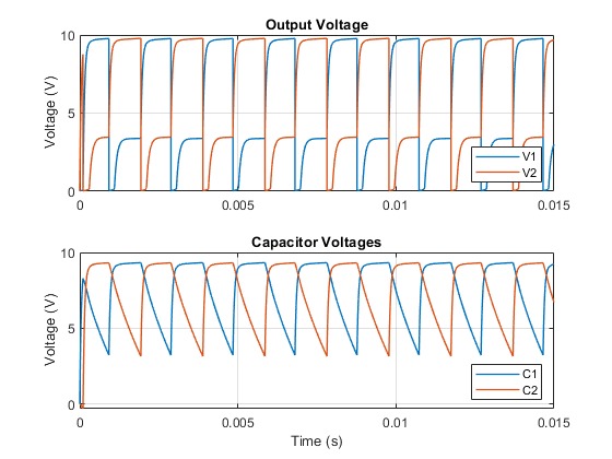
Simulation Results from Simscape Logging
The plots below show voltages in the astable oscillator circuit. The charging and discharging of capacitors C1 and C2 turns the transistors on and off.
