Clock Domain Crossing Using the HDL Dual Clock FIFO Block
R2026bThis example shows how to use the HDL Dual Clock FIFO example library block to approximate the functional behavior of a dual-clock first-in first-out (FIFO) and transfer data between two independent clock domains. The block captures data ordering, flag behavior, and backpressure during simulation.
Modeling Requirements
To perform clock domain crossing by using the HDL Dual Clock FIFO block, you must model the design to run at the clock rate. When you use the block in your device under test (DUT):
The write domain inputs,
WrDataandWrEnable, must use the same sample rate.WrDatacannot inherit its rate because the block uses this rate to propagate the write domain timing.The read domain sample rate, such as the rate of
RdEnable, must be different from the write domain rate for code generation.You must specify the read domain sample rate either by connecting
RdEnableat the desired rate or by setting the Read sample time mask parameter.The HDL Dual Clock FIFO block mask parameters control the XPM configuration, including the FIFO depth, the operating mode (classic or first-word fall-through), and the number of cycles of simulated reset-busy latency. The FIFO depth must be a power of two and greater than or equal to sixteen.
The HDL Dual Clock FIFO block does not reproduce cycle-accurate timing or gray-coded pointer details. You must configure the Simulink® sample rates to match the actual hardware clock rates so that the block correctly represents the relationship between the write and read domains.
Limitations
When you target the AMD® platform with Verilog® as the target language, HDL Coder™ instantiates the AMD Xilinx Parameterized Macro (XPM) asynchronous
FIFO (xpm_fifo_async) in place of the HDL Dual Clock FIFO block, giving you
a device-optimized implementation with vendor timing constraints.
When using the HDL Dual Clock FIFO block:
The Language model configuration parameter must be
Verilog.The Synthesis Tool model configuration parameter must be
Xilinx Vivado.The Clock inputs model configuration parameter must be
Multiple.
Transfer Data Across Clock Domains by Using the HDL Dual Clock FIFO Block
In this example, you:
Use the HDL Dual Clock FIFO block to cross clock domains when modeling at clock rate.
Generate a multiple-clock HDL IP core by using HDL Coder™.
Integrate the generated IP core into an AMD Vivado™ project and deploy it to a ZedBoard™.
Use FPGA I/O to test the design on hardware.
Prerequisites
To interact with the deployed IP core, you must:
Install the SoC Blockset™ (for AMD) Support Package. For details, see Install Support for AMD FPGA and SoC Devices (SoC Blockset).
Download the MathWorks® firmware image on the ZedBoard™ SD card. To learn how to set up the SD card, see Set Up Custom Boards Using the Hardware Setup (SoC Blockset).
Examine the Model
When you model multiple-clock designs in Simulink®, you represent each clock domain by a unique sample rate. To model data transfers between clock domains, the sample rates must match the frequencies of the corresponding hardware clocks. The hdlcAsyncFIFO model compares two ways of crossing the sample-rate boundary: the withDualClockFIFO subsystem and the withoutDualClockFIFO subsystem.
Open the HDLDUT subsystem in the example model.
load_system("hdlcAsyncFIFO");
open_system("hdlcAsyncFIFO/HDLDUT");
set_param("hdlcAsyncFIFO","SimulationCommand","Update")
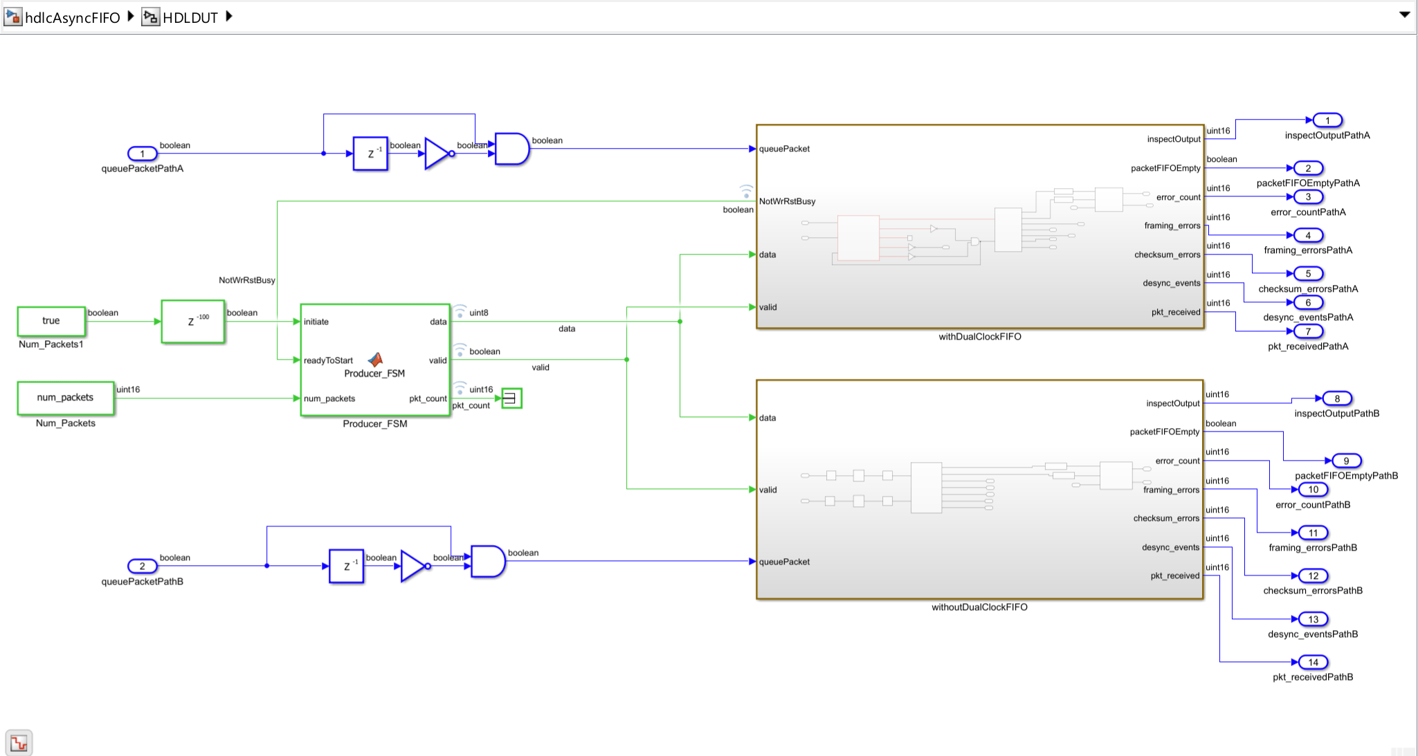
The HDLDUT subsystem contains a producer that drives the same data through two parallel clock-domain-crossing paths into matching consumers. The model uses two clock domains with sampling times and packet count defined in the model initialization callback. Ts1 = 1/100e6 is the fast, 100 MHz domain. Ts2 = 1/77e6 is the slow, 77 MHz domain. num_packets = uint16(100) sets the number of packets per burst.
Examine the Producer_FSM Block
The Producer_FSM subsystem is a finite state machine (FSM) that runs in the fast clock domain, Ts1, and generates framed packets at an effective rate of 50 MHz. It sends one byte every two 100 MHz cycles and num_packets packets per burst. Each packet carries a payload byte from a counter that starts at 2, increments by 1 per packet, and wraps at 170 (0xAA). Each packet is five bytes:
Position | Name | Value |
1 | SOP |
|
2 | PL | Lower 8 bits of 16-bit counter |
3 | PH | Upper 8 bits of 16-bit counter |
4 | Checksum |
|
5 | EOP | |
The Producer_FSM subsystem outputs data to two subsystems, withDualClockFIFO and withoutDualClockFIFO. Each subsystem contains a consumer that decodes the packets.
Examine the withDualClockFIFO Subsystem
The withDualClockFIFO subsystem writes data through the HDL Dual Clock FIFO block to cross from the 100 MHz write domain to the 77 MHz read domain. The HDL Dual Clock FIFO block outputs a value and asserts the valid signal whenever it is not empty. Then the consumer block decodes the data.
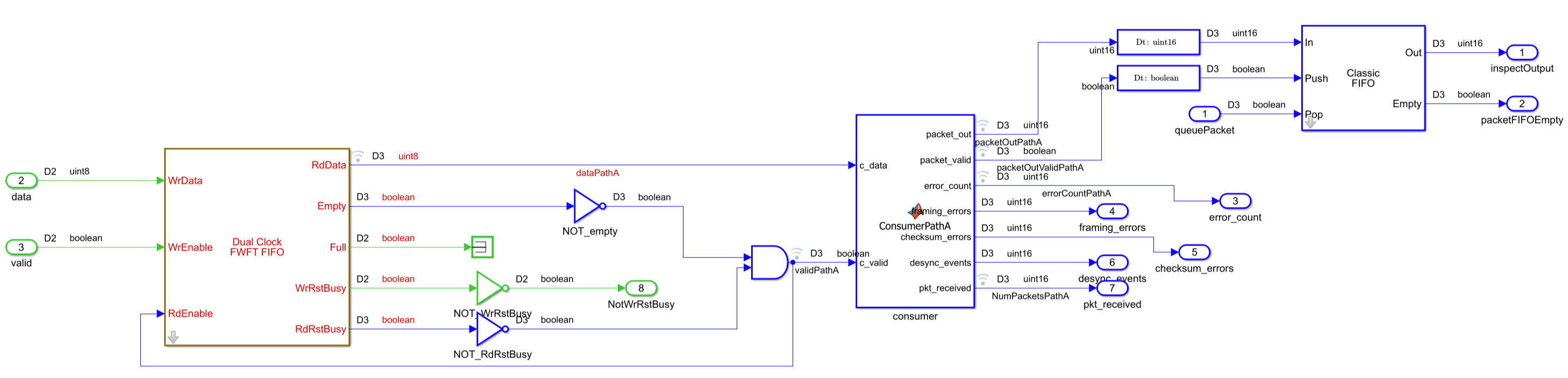
The HDL Dual Clock FIFO block configuration is:
Write depth: 256
Data width: 8 bits
Read mode: First-Word Fall-Through (FWFT)
Write clock: 100 MHz producer domain (
Ts1)Read clock: 77 MHz consumer domain (
Ts2)
Because the HDL Dual Clock FIFO block targets AMD devices, its interface matches the AMD xpm_fifo_async primitive. The block has two reset-busy outputs: WrRstBusy and RdRstBusy. Each signal indicates when its clock domain is resetting. The design must wait for these signals to go low before sending or receiving data.
The Producer_FSM subsystem waits for two things before it starts transmitting. The first is the NotWrRstBusy flag, which is the inverted WrRstBusy flag from the FIFO, available at the top of the withDualClockFIFO subsystem. It goes high once the write side finishes resetting. The second is initiate, a startup delay created by taking a constant true and delaying it by 100 fast-clock cycles.
When you use multiple rates as multiple clocks, resets are not modeled explicitly. The delay register inherits the reset of its clock domain, which is the same reset that resets the FIFO write side, and the 100-cycle countdown begins when the write clock domain comes out of reset.
Typically, WrRstBusy goes low within a few write-clock cycles after reset. Because the 100-cycle initiate delay is longer than that, it is always the slower of the two conditions. This delay provides the producer with a safety margin before it drives the data.
Examine the withoutDualClockFIFO Subsystem
The withoutDualClockFIFO subsystem passes data from the Producer_FSM subsystem through two Unit Delay blocks, which act as a dual-register synchronizer, into a consumer subsystem. This path is intentionally unreliable. Without a FIFO, there is no flow control and no guarantee that every byte reaches the consumer. Additionally, because the two clocks originate from independent sources, the multi-bit data bus is subject to metastability when sampled by the destination clock.
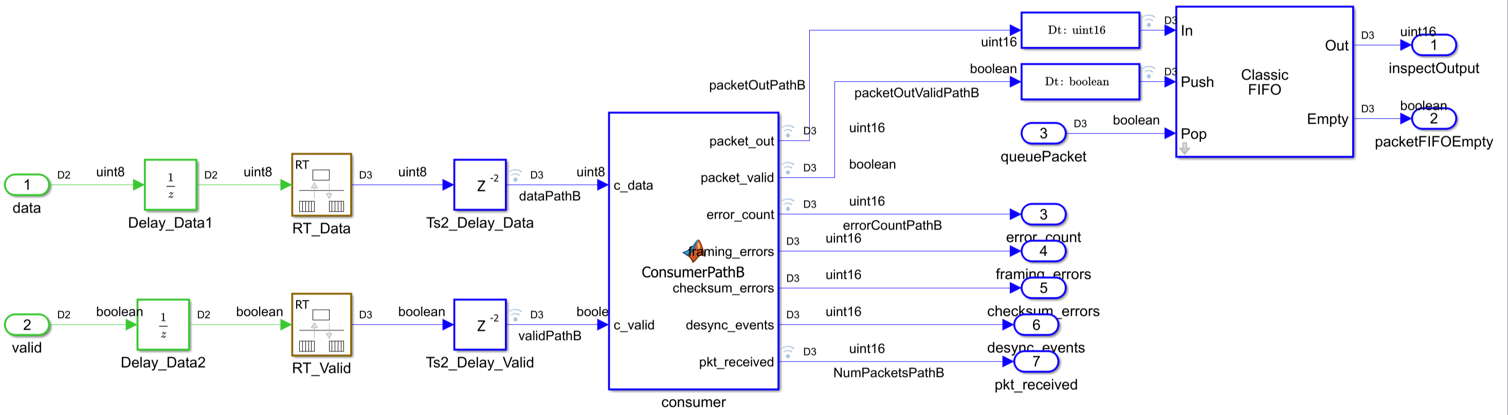
Examine the consumer Subsystems
Both subsystems contain the consumer subsystem. It decodes the five-byte packets, validates the checksum and framing, and produces these outputs:
pkt_received— Number of successfully validated packetserror_count— Total errors detectedframing_errors— Invalid EOP markerschecksum_errors— Payload checksum mismatchesdesync_events— Unexpected bytes received while waiting for SOP
After the consumer block validates a packet, it stores the reconstructed 16-bit payload in a single-clock output FIFO that you can read by using AXI4-Lite registers. The queuePacketPathA and queuePacketPathB signals pop one value from each output FIFO. When the AXI4-Lite register transitions from true to false, it generates a single-cycle pulse. This pulse generation logic is in the design under test (DUT).
Simulate the Model
Verify the functional behavior of the DUT by simulating the model. While behavioral simulation cannot model metastability, it can verify packet framing, checksum logic, and FIFO handshaking.
sim("hdlcAsyncFIFO");
After the simulation completes, open the Logic Analyzer by clicking Logic Analyzer on the Simulation tab. The model logs the data and valid signals at the output of the producer and at the input of each consumer subsystem.
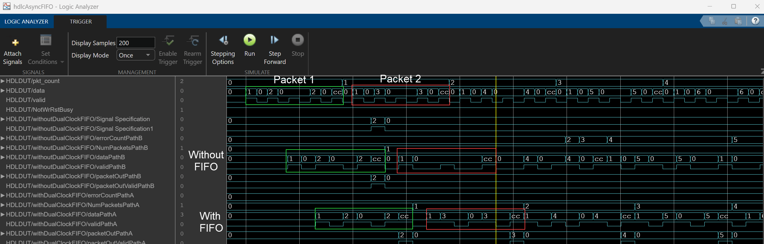
Both subsystems sample the first packet correctly, but the withoutDualClockFIFO subsystem contains errors in later packets. For example, the withoutDualClockFIFO subsystem samples only the SOP and EOP. Because the consumer subsystem expects four valid elements between SOP and EOP, it misinterprets the EOP as a payload byte and desynchronizes for several subsequent transfers.
The root cause is a data coherency problem. In the withoutDualClockFIFO subsystem, the producer asserts data and valid at an effective rate of 50 MHz on a 100 MHz clock. These signals pass through a register in the 100 MHz domain, then through two registers in the 77 MHz consumer subsystem domain. Because 77 MHz and 100 MHz are unrelated frequencies, the 77 MHz clock can miss a valid pulse entirely. The pulse is only 10 ns wide, which is shorter than the 77 MHz clock period (~13 ns) time period, if no rising edge falls within that window the byte is lost. This causes the consumer to miss bytes and lose packet alignment.
Generate HDL IP Core
Generate a generic HDL IP core from the HDLDUT subsystem. In this example, you generate an IP core for a generic AMD platform. First, set up the Xilinx Vivado synthesis tool path by using the hdlsetuptoolpath function. Use your own Vivado installation path.
hdlsetuptoolpath("ToolName","Xilinx Vivado","ToolPath","C:\Xilinx\Vivado\2025.1\bin\vivado.bat")
Then, configure the model for IP core generation:
In the Apps tab, click HDL Coder. In the HDL Code tab, in the Output section, set the button to IP Core. Set Code for to
HDLDUT.Click Settings to open the Configuration Parameters dialog box. In the HDL Code Generation > Target pane, set Project Folder to
hdl_prj, set Target Platform toGeneric Xilinx Platform, and set Synthesis Tool toXilinx Vivado.Click Settings > HDL Code Generation. In the Global Settings pane, set Clock inputs to
Multiple.
Next, map the DUT ports to the IP core interfaces. In this example, map all DUT ports to AXI4-Lite interfaces:
In the IP Core pane, select the Interface Mapping tab. If the mapping table does not appear, click the Reload IP core settings
 button to compile the model and populate the DUT ports and their data types.
For all ports, set the Interface to
AXI4-Lite.Validate your settings by clicking the Validate IP core settings
 button.
In the HDL Code tab, click Generate IP Core. After generation completes, the IP core report opens and displays details about the multiple-clock connections, the generated clock ports, and the AXI4-Lite register map. Inspect the generated HDL code for the DUT subsystem. The xpm_fifo_async instantiation with the values configured in the model: depth of 256, data width of 8 bits, and FWFT read mode, the code is instantiated in hdl_prj\hdlsrc\hdlcAsyncFIFO\HDLDUT_ip_src_HDL_Dual_Clock_FIFO.v. To learn how to configure the model for IP core generation and map the IP core interfaces using the HDL Coder Toolstrip, see Get Started with IP Core Generation from Simulink Model.
 xpm_fifo_async #(.CASCADE_HEIGHT(0),
                   .CDC_SYNC_STAGES(2),
                   .DOUT_RESET_VALUE("0"),
                   .ECC_MODE("no_ecc"),
                   .EN_SIM_ASSERT_ERR("warning"),
                   .FIFO_MEMORY_TYPE("auto"),
                   .FIFO_READ_LATENCY(1),
                   .FIFO_WRITE_DEPTH(256),
                   .FULL_RESET_VALUE(0),
                   .PROG_EMPTY_THRESH(10),
                   .PROG_FULL_THRESH(10),
                   .RD_DATA_COUNT_WIDTH(1),
                   .READ_DATA_WIDTH(8),
                   .READ_MODE("fwft"),
                   .RELATED_CLOCKS(0),
                   .SIM_ASSERT_CHK(0),
                   .USE_ADV_FEATURES("0707"),
                   .WAKEUP_TIME(0),
                   .WRITE_DATA_WIDTH(8),
                   .WR_DATA_COUNT_WIDTH(1))
Integrate the Generated HDL IP Core into an AMD Vivado SoC Project
To use the generic IP core as part of a larger system, create a Vivado project, integrate the IP core, and generate a bitstream for the ZedBoard. This image shows the connections in the Vivado block design. The first clock is derived from the Zynq Processing System clock (FCLK_CLK0, 100 MHz) and routed through a Clock Wizard that generates the 77 MHz consumer domain frequency.
The second clock is a fixed 100 MHz clock from the on-board crystal oscillator, brought into the programmable logic (PL) through the Xilinx Design Constraints (XDC) constraints file, and serves as the producer domain clock. For a detailed walkthrough of manual IP core integration in Vivado, see Generate Clock-Domain-Crossing Pulse Synchronizer by Generating a Multiple-Clock IP Core.
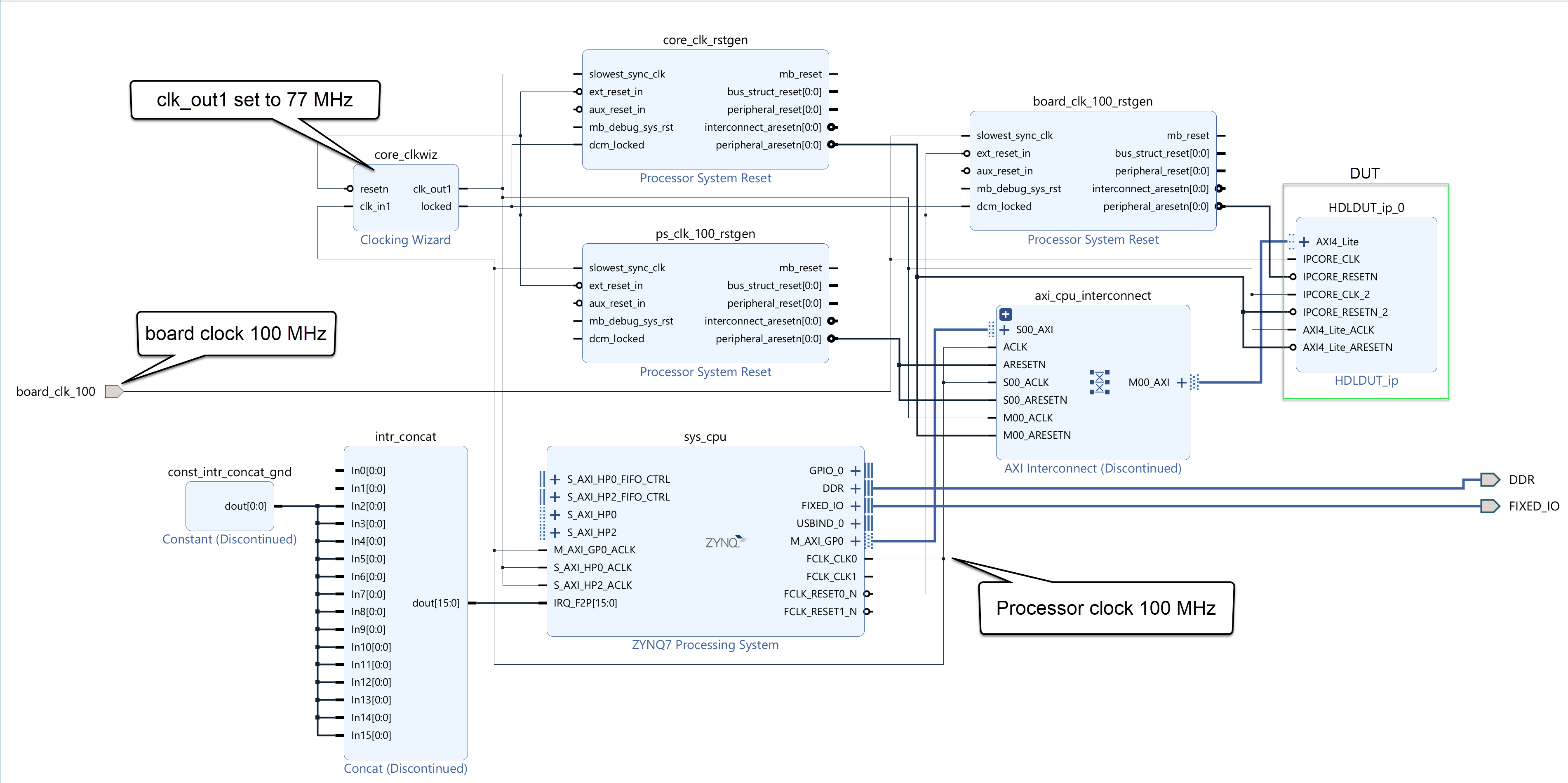
This example includes Tcl scripts that automate project creation, block design assembly, IP insertion, clock and reset connections, and bitstream generation. The integration uses three files:
vivado_custom_design.tcl— Tcl file that creates the base block design containing the Zynq Processing System (PS), AXI interconnect, Clock Wizard, and reset generators. This file was created by using Vivado 2025.1.1.board_clk_100.xdc— Constraints file that maps the 100 MHz oscillator on the ZedBoard to theboard_clk_100port in the block design.build_custom_prj.tcl— Top-level script that creates the Vivado project in a newhdl_fifofolder, sources the block design, adds the generated IP core to the IP catalog, instantiates it in the block design, connects clocks and resets, adds timing constraints, and runs synthesis and implementation.
To create the project and build the bitstream, run:
!vivado -source build_custom_prj.tcl &
Interact with the FPGA Design by Using MATLAB
To compare error statistics between the withDualClockFIFO and withoutDualClockFIFO subsystems on real hardware, use an fpga object to interact with the deployed design.
Program the FPGA hardware with the generated bitstream and configure the processor with the corresponding device tree. The device tree devicetree_axilite_iio.dtb is available in the firmware image when you configure your board using the Hardware Setup app. When you use build_custom_prj.tcl for integration, the bitstream is in the hdl_fifo project folder.
hProcessor = xilinxsoc();
programFPGA(hProcessor, ...
    "hdl_fifo\hdl_fifo.runs\impl_1\system_top_wrapper.bit", ...
    remoteFile("devicetree_axilite_iio.dtb"));
Open and run the custom_interface_visualize.m script. The script creates an fpga object, configures the AXI4-Lite interfaces to interact with the DUT ports of the deployed IP core, reads the error counters from both paths, retrieves the packet payloads, and prints a side-by-side comparison.
run("custom_interface_visualize")
The script prints a formatted summary comparing both paths:
==============================================================
  CDC Path Comparison - Producer/Consumer Results
  Path A: Async FIFO (proper CDC)
  Path B: Dual-Register (no CDC)
==============================================================

                                 Path A     Path B
                                 (FIFO) (Dual-Reg)
  ------------------------------------------------
  Packets Received                  100         20
  Total Errors                        0        151
  Framing Errors                      0         40
  Checksum Errors                     0         30
  Desync Events                       0         81
  FIFO Empty                      false      false

  ------------------------------------------------
  Dequeued Payloads:
                                 Path A     Path B
  Packet 1                            2          4
  Packet 2                            3          9

  ------------------------------------------------
  Verdict:
  Path A (FIFO):      PASS - 100/100 packets, 0 errors
  Path B (Dual-Reg):  FAIL - 20/100 packets, 151 errors
     CDC errors expected - demonstrates why async FIFO is needed.

==============================================================
The withDualClockFIFO subsystem receives all 100 packets with 0 errors, and the retrieved payloads are consecutive, which confirms that the FIFO preserved the data integrity and ordering across the clock domains. The withoutDualClockFIFO subsystem receives fewer than 100 valid packets, which contains framing errors, checksum errors, and desynchronization events. The retrieved payloads are non-consecutive, which demonstrates that the dual-register approach does not reliably transfer multi-byte streaming data across asynchronous clock domains.
On real hardware, the results from the withoutDualClockFIFO subsystem differ from the simulation results for these reasons:
In Simulink®, the two clocks always start with a fixed, deterministic phase relationship, so the simulation misses the same bytes on every run. On hardware, the clocks come from independent sources and their relative phase is arbitrary at power-up and can drift over time, so different bytes are missed on each run and the error counts might not be repeatable.
Metastability can corrupt the sampled data values when a clock edge falls during the setup of a flip-flop or hold window.
This contrast confirms that for continuous or burst data transfers between asynchronous clock domains, a dual-clock FIFO is essential. Simple register synchronizers are only suitable for single-bit level signals or pulses with adequate spacing.

