FIL Simulation with HDL Workflow Advisor for Simulink
Step 1: Start HDL Workflow Advisor
Follow instructions for invoking the HDL Workflow Advisor. See Getting Started with the HDL Workflow Advisor (HDL Coder).
Note
You must have an HDL Coder™ license to generate HDL code using the HDL Workflow Advisor.
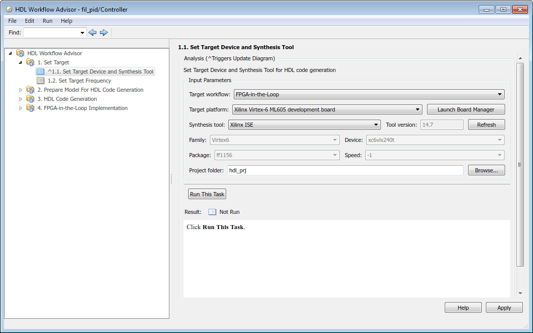
Step 2: Set Target and Target Frequency
At step 1, Set Target, click 1.1 Set Target Device and Synthesis Tool and do the following:
Select
FPGA-in-the-Loopfrom the pull-down list at Target workflow.Under Target platform, select a development board from the pull-down list. Family, Device, Package, and Speed are filled in by the HDL Workflow Advisor. If you have not yet downloaded an HDL Verifier™ FPGA board support package, select
Get more boards. Then return to this step after you have downloaded an FPGA board support package.For Project folder, enter the folder name to save the project files into. The default is
hdl_prjunder the current working folder.
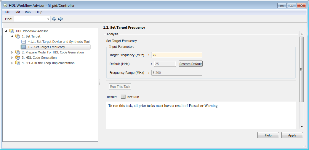
After you select a FIL target in Step 1.1, click 1.2 Set Target Frequency.
Set the Target Frequency (MHz) for the clock speed of your design implemented on the FPGA. The available range of frequencies is shown in the Frequency Range (MHz) parameter. For Intel® boards and AMD® boards, Workflow Advisor checks the requested frequency against those possible for the requested board. If the requested frequency is not possible for this board, Workflow Advisor returns an error and suggests an alternate frequency. For AMD Vivado®-supported boards, or PCI Express® boards, Workflow Advisor cannot check the frequency. The synthesis tools make a best effort attempt at the requested frequency but might choose an alternate frequency if the specified frequency was not achievable. The default is
25MHz.
Step 3: Prepare Model for HDL Code Generation
At step 2, Prepare Model for HDL Code Generation, perform step 2.1 as described in Prepare Model for HDL Code Generation Overview (HDL Coder).
In addition, perform step 2.2 Check FPGA-in-the-Loop Compatibility to verify that the model is compatible with FIL.
Note
If your HDL module includes a black box with a clock enable, you must clear the
Minimize clock enable configuration parameter. For more information, see
Minimize clock enables (HDL Coder).
Step 4: HDL Code Generation
At step 3, HDL Code Generation, perform steps 3.1 and 3.2 as described in HDL Code Generation Overview (HDL Coder).
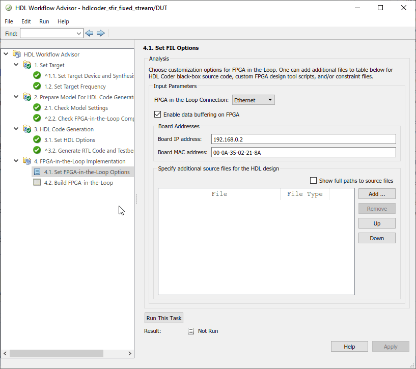
Step 5: Set FPGA-in-the-Loop Options
At step 4.1, Set FPGA-in-the-Loop Options, change these options if necessary:
FPGA-in-the-Loop Connection: Select the FIL simulation connection method. The options in the drop-down menu update depend on the connection methods supported for the target board you selected. If the target board and HDL Verifier support the connection, you can choose
Ethernet,JTAG,PCI Express, orUSB Ethernet.MATLAB/FPGA Synchronization Mode: Select a mode for streaming data between MATLAB® and the DUT. If the target board and FIL connection support, you can choose one of these modes:
Lockstep — In this mode, the DUT on the FPGA operates in lockstep with MATLAB. This mode is the default option and it is implicit in FIL simulation.
Free-running FPGA — In this mode, the DUT on the FPGA runs asynchronously with MATLAB. The hardware clock runs continuously inside the FPGA itself.
Note
This mode works only when you use FIL with a MATLAB System object™. It does not work when you use FIL with a Simulink® block.
For more information on these modes, see What Is Free-Running FPGA-in-the-Loop?.
Generate host interface script: Select this option to generate a host interface script,
gs_, whereDUTName_interface_fil.mDUTNamefilObjobject for interfacing with the FPGA from MATLAB. The interface script contains MATLAB commands that connect to the hardware and program the FPGA, and examples of how to exchange data with your algorithm as it runs on the hardware.Enable data buffering on FPGA: Select this option to enhance simulation performance. When selected, FIL utilizes BRAMs on the FPGA to buffer Ethernet packets in frame-based processing mode. Clear this parameter when BRAM resources are scarce in your design. Available for Ethernet connection only.
Board Address:
When you select an Ethernet connection for an FPGA board, you can adjust the board IP and MAC addresses, if necessary. If the board includes a processing unit, use the Guided Hardware Setup to configure the SD card.
Option Instructions Board IP address Use this option for setting the IP address of the board if it is not the default IP address (192.168.0.2).
If the default board IP address (192.168.0.2) is in use by another device, or you need a different subnet, change the Board IP address according to the following guidelines:
The subnet address, typically the first three bytes of board IP address, must be the same as the subnet of the host IP address.
The last byte of the board IP address must be different from the last byte of the host IP address.
The board IP address must not conflict with the IP addresses of other computers.
For example, if the host IP address is 192.168.8.2, then you can use 192.168.8.3, if available.
Board MAC address Under most circumstances, you do not need to change the board MAC address. If you connect more than one FPGA development board to a single host computer, change the board MAC address for any additional boards so that each address is unique. You must have a separate NIC for each board.
To change the Board MAC address, click in the Board MAC address field. Specify an address that is different from that belonging to any other device attached to your computer. To obtain the Board MAC address for a specific FPGA development board, refer to the label affixed to the board or consult the product documentation.
Specify additional source files for the HDL design:
Indicate additional source files for the DUT using Add. To (optionally) display the full paths to the source files, check the box titled Show full paths to source files. The HDL Workflow Advisor attempts to identify the source file type. If the file type is incorrect, you can change it by selecting from the File Type drop-down list.
FIL Options
Step 6: Set DUT I/O Ports
This step is enabled only when you select the free-running FPGA mode.
At step 4.2, Set DUT I/O Ports, the HDL Workflow Advisor parses the input and output ports of your DUT from the top file. It infers each port type from the HDL port name. Verify and modify the port type as needed.
Step 7: Generate FPGA Programming File, FIL Model, and Host Interface Script
At step 4.3 (4.2 for lockstep mode), Build FPGA-in-the-Loop, click Run this task.
During the build process, the following actions occur:
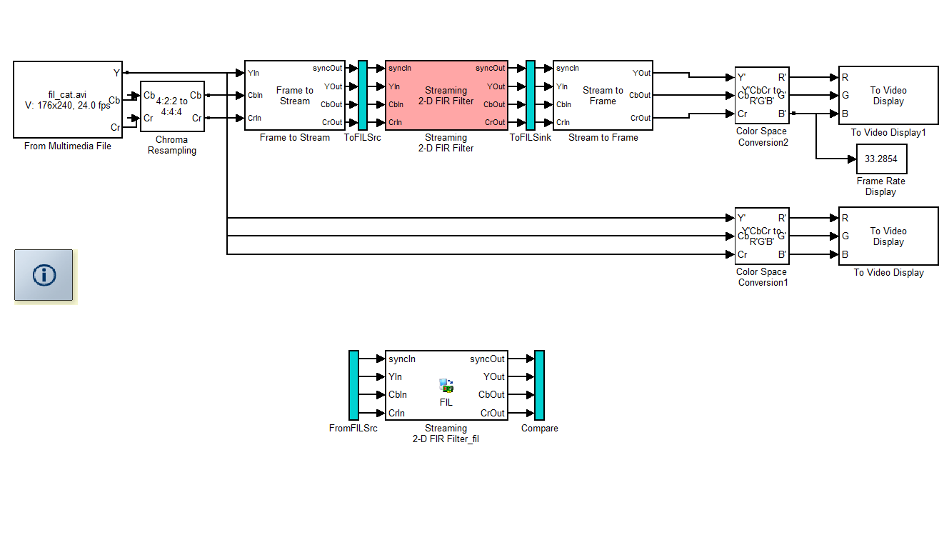
Lockstep mode only — The HDL Workflow Advisor generates a FIL block named after the top-level module and places it in a new model. The next figure shows an example of the new model containing the FIL block.
Note
For free-running FIL, the HDL Workflow Advisor does not generate the Simulink verification model, as this mode works only when you use FIL with a MATLAB System object. It does not work when you use FIL with a Simulink block.
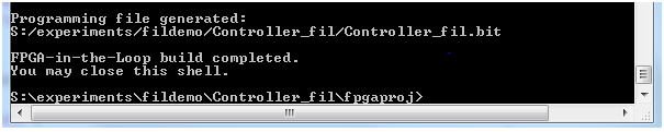
After new model generation, the HDL Workflow Advisor opens a command window:
In this window, the FPGA design software performs synthesis, fit, PAR, and FPGA programming file generation.
When the process completes, a message in the command window prompts you to close the window.
Lockstep mode only — The HDL Workflow Advisor builds a testbench model around the generated FIL block.
The HDL Workflow Advisor generates a host interface script for interfacing with the FPGA from MATLAB if you select the Generate host interface script option in step 4.1.
Step 7: Load Programming File onto FPGA
Ensure your FPGA development board is set up, powered on, and connected to your machine as directed by the board manufacturer documentation. Then, perform the following steps to program the FPGA:
Double-click the FIL block in your Simulink model to open the block mask.
On the Main tab, click Load to download the programming file to the FPGA.
The load process may take several minutes, depending on how large the subsystem is. For very large subsystems, the process can take an hour or longer.
Alternatively, you can use the generated host interface script,
gs_, to program the
FPGA.DUTName_interface_fil.m
For further troubleshooting tips, see Load Programming File onto FPGA.
Step 8: Run Simulation
In Simulink, on the Simulation tab, click Run. The results of the FIL simulation should match those of the Simulink reference model or of the original HDL code.
Note
Regarding initialization: Simulink starts from time 0 every time, which means the RAM in Simulink is initialized to zero. However, this is not true in hardware. If you have RAM in your design, the first simulation will match Simulink, but any subsequent runs may not match.
The workaround is to reload the FPGA bitstream before re-running the simulation. To do this, click Load on the FIL block mask.