Design and Implement Delta-Sigma Modulator using Switched-Capacitor Integrator
This example shows how to use the Delta Sigma Modulator Block to include a physically realizable switched-capacitor (SC) based discrete-time integrator from Mixed-Signal Blockset™. The objective is to bridge the gap between behavioral modeling and circuit-level implementation. By utilizing the Mixed-Signal Blockset™, this example demonstrates that a practical DSM ADC can be accurately modeled to achieve SNR and ENOB metrics comparable to commercial hardware, such as the ADS1209 [1] which is used as a reference for this example.
Ideal Behavioral Model
The Delta Sigma Modulator block from Mixed-Signal Blockset uses ideal Discrete Filter block as demonstrated in the MATLAB example - Delta Sigma Modulator Data Converter with Half-Band Filter for Decimation. This block is a mathematical IIR filter that represents the system-level behavior of the modulator. It is useful for algorithm prototyping and estimating the ideal performance of a given DSM architecture or topology. However, it does not account for circuit-level non-idealities such as OTAs, switches, comparators, parasitics, clock jitter, or thermal noise. These factors ultimately limit performance in silicon implementations. To address this limitation, this example demonstrates how to use a switched-capacitor circuit-based representation of the discrete-time integrator block from the Mixed-Signal Blockset.
The image below shows the output of a discrete sinusoidal signal passed through an ideal Discrete Filter block and a Discrete-Time Integrator (DT Integrator) block. Note that for Discrete Filter block, the output amplitude can grow much larger than what the SC‑aware DT Integrator produces.
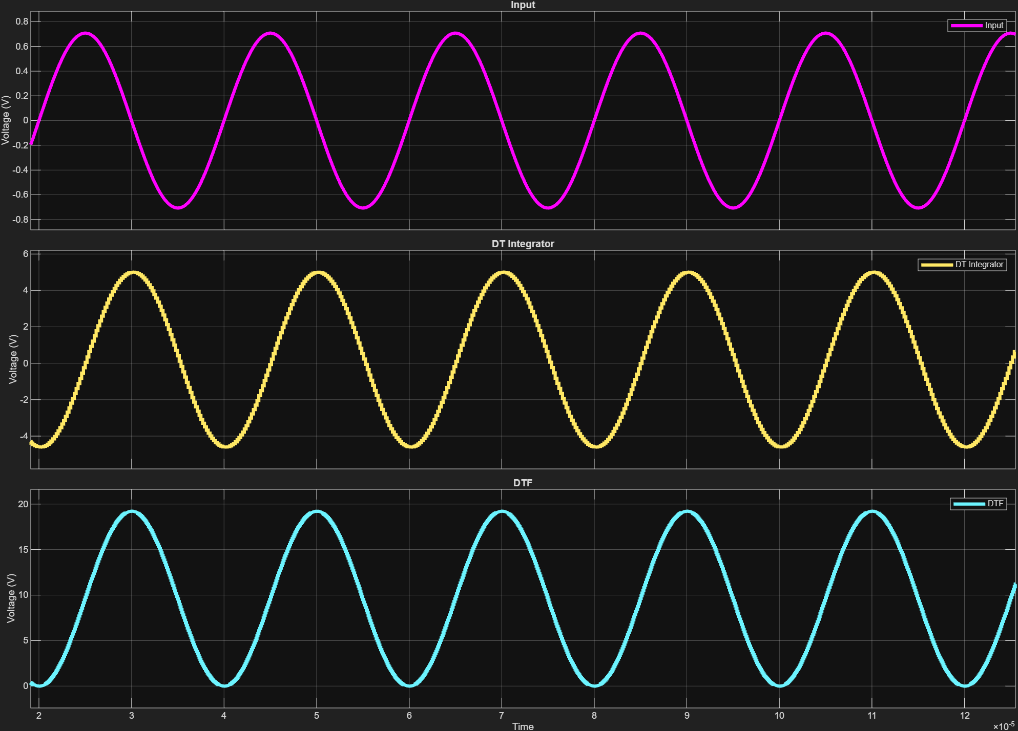
The Discrete Filter block implements an ideal IIR transfer function with unlimited numerical precision and no physical constraints. In contrast, the DT Integrator models a charge-redistribution switched-capacitor SC circuit.
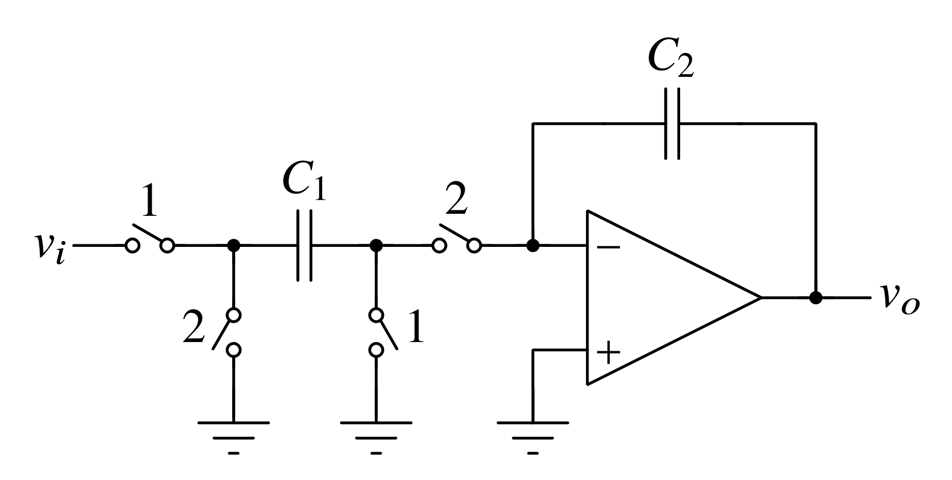
The gain is determined by capacitor ratios (), and output swing is limited by supply voltage and circuit parasitics. A typical DT Integrator () is a SC based integrator which realizes the following transfer function:
where and are sampling and integration capacitors, respectively. The above transfer function represents a one-tick delayed accumulator whose per-cycle gain comes from capacitor ratio, not a direct numeric scale, bounded by loop scaling and device limits (scaling at ).
SC integrators provide an accurate and robust way to implement discrete-time integration in CMOS technology. The example focuses on the switched-capacitor integrators as the building block for our DSM. SC integrators offer several advantages: they use capacitor ratios to define integration coefficients (very robust against absolute process variation), are naturally compatible with sampled-data systems, and can be accurately modeled with parasitics, noise, and nonlinearity. The following sections derive the theoretical performance limits and show how design choices like Oversampling Ratio (OSR), DSM loop-filter order, component sizing directly impact the Signal-to-Noise Ratio (SNR) and Effective Number of Bits (ENOB).
Replacing Discrete Filter with DT Integrator in Delta-Sigma Modulator
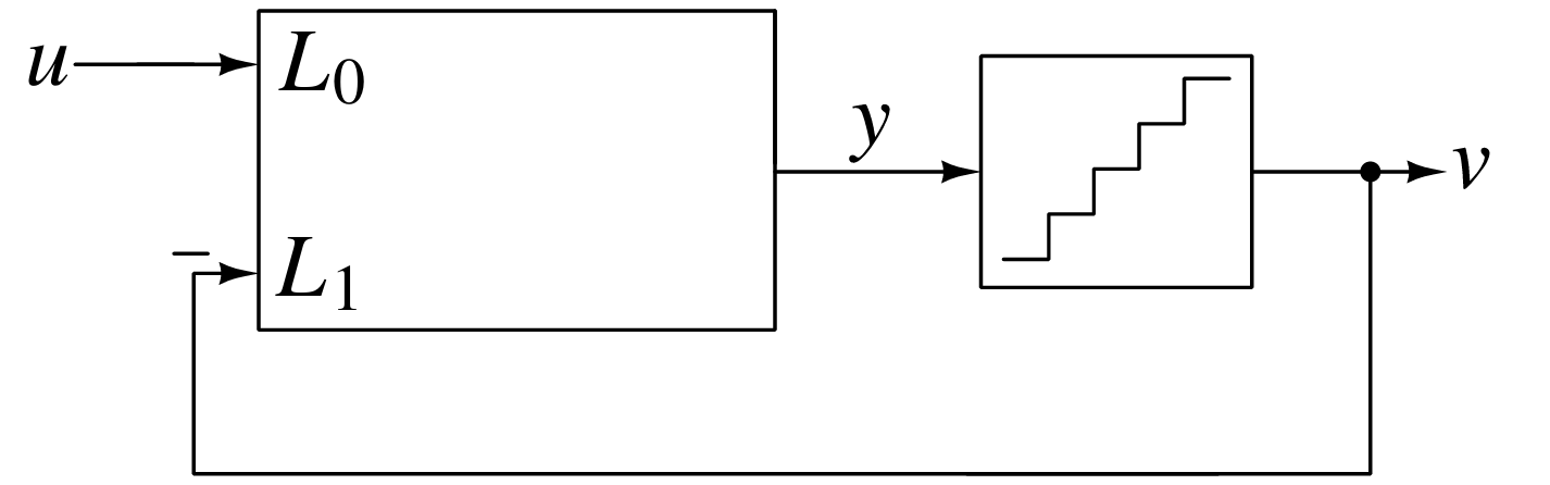
Mixed-Signal Blockset provides an ideal configurable Delta Sigma Modulator block that supports various DSM topologies like Cascade of resonators or integrators in feedback or feedforward configuration (CIFB, CRFB, CIFF, and CRFF). You can use these topologies to create DSM-based ADC architectures with orders ranging from 2 to 6. After configuring the DSM with a specific architecture, order and OSR, you can select Edit System in the block parameters dialog box to modify to create SC‑based DSM design:
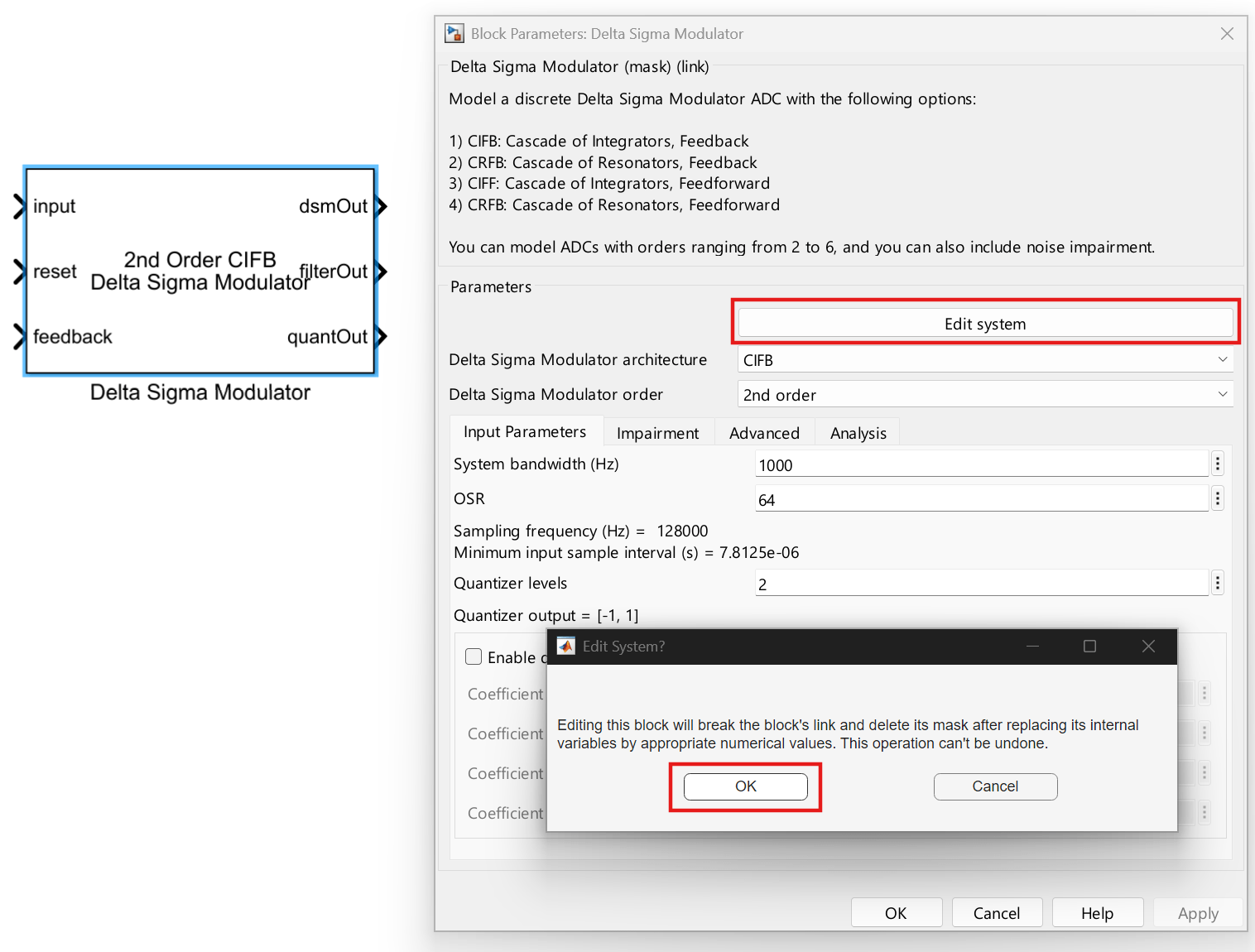
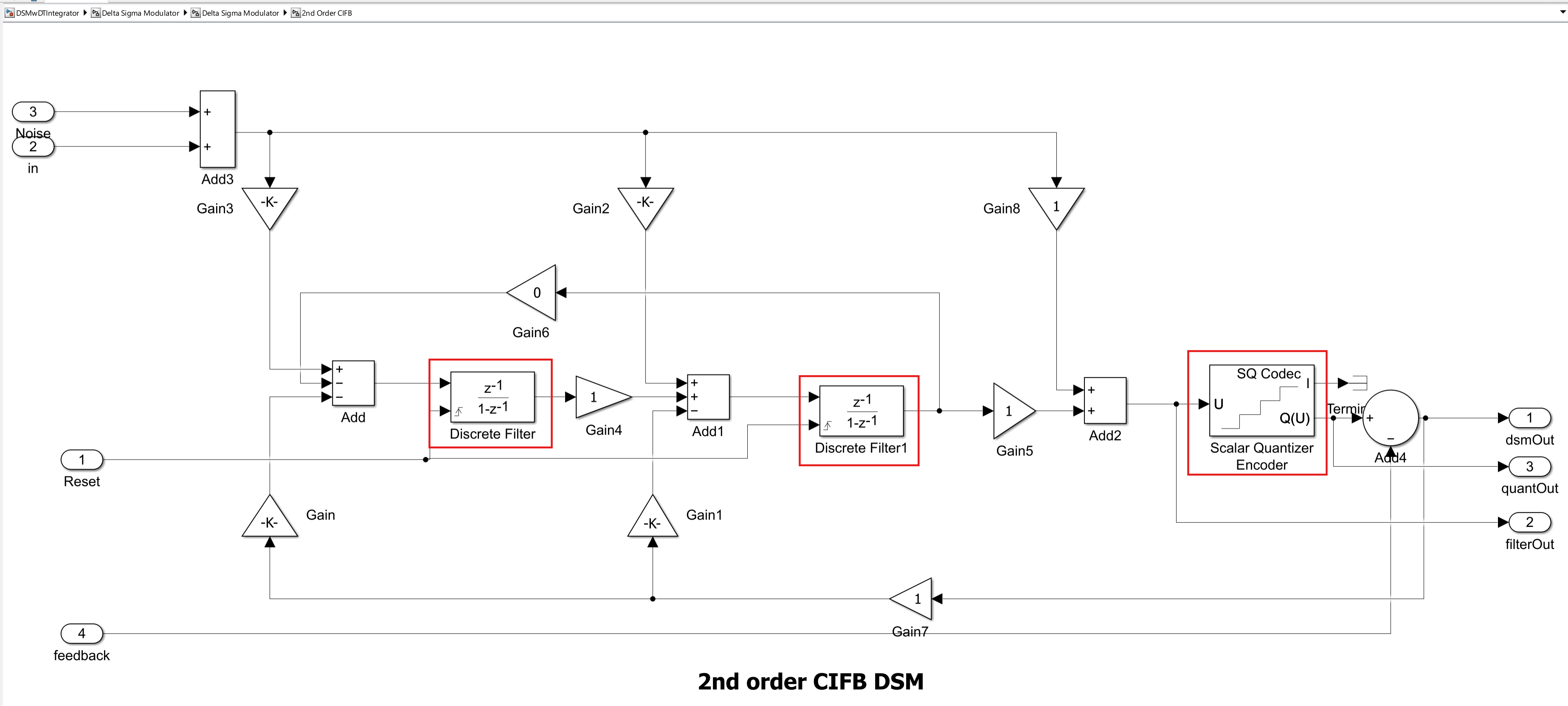
To implement a realistic model of a DSM which includes circuit-level non-idealities, you can replace each Discrete Filter block with a DT Integrator block from Mixed-Signal Blockset. You can replace the Scalar Quantizer Encoder block with Quantizer block also coming from Mixed-Signal Blockset. The Quantizer block lets you model gain error, offset error, and INL impairments in the modulator loop and is based on assumption that the input signal exciting the quantizer does not overload it.
This example focuses on modeling Texas Instrument’s DSM based ADC part i.e., TI ADS1209. This has a CIFB (Cascade of Integrators with distributed FeedBack) topology as it offers good stability margins and straightforward component scaling.
Choosing Realization Coefficients (a, g, b, c)
The loop's internal headroom and quantizer input margin depend on how the behavioral NTF/STF are realized as a state-space (ABCD) network and then mapped to a CIFB structure[2]. The ABCD matrices form the mathematical blueprint of the modulator architecture by describing exactly how signals flow into, through, and out of the cascade of integrators.
Each integrator stage in a delta‑sigma loop adds up several signals. The coefficients b, c, a, and g are simply the gains that determine how strongly each signal contributes at that summing node. They control the shape of the NTF and STF by defining the loop gain, the feedforward paths, and the DAC feedback strength. The sets (a,g,b,c) express the same system as the ABCD matrices, but in a form that matches standard ΔΣ modulator topologies. All of these coefficient sets, along with the ABCD state‑space description, are generated by Mixed‑Signal Blockset functions such as synthesizeSTF, realizeNTF, stuffABCD, and mapABCD.
For all the architectures available in the Delta Sigma Modulator block, the default feed-in (or feedback) coefficients (e.g., ) originate from the behavioral design flow using Schreier’s Delta Sigma Toolbox - now a part of MALTAB Mixed-Signal Blockset. These coefficients are optimized to keep internal integrator states and the quantizer input within safe bounds in an idealized model. They do not inherently account for SC capacitor ratio limits or OTA performance constraints unless you explicitly configure them to do so.
When you implement a physically realizable SC loop, the behavioral coefficients must be mapped to match the ratios of each integrator stage while preserving the synthesized NTF and STF.
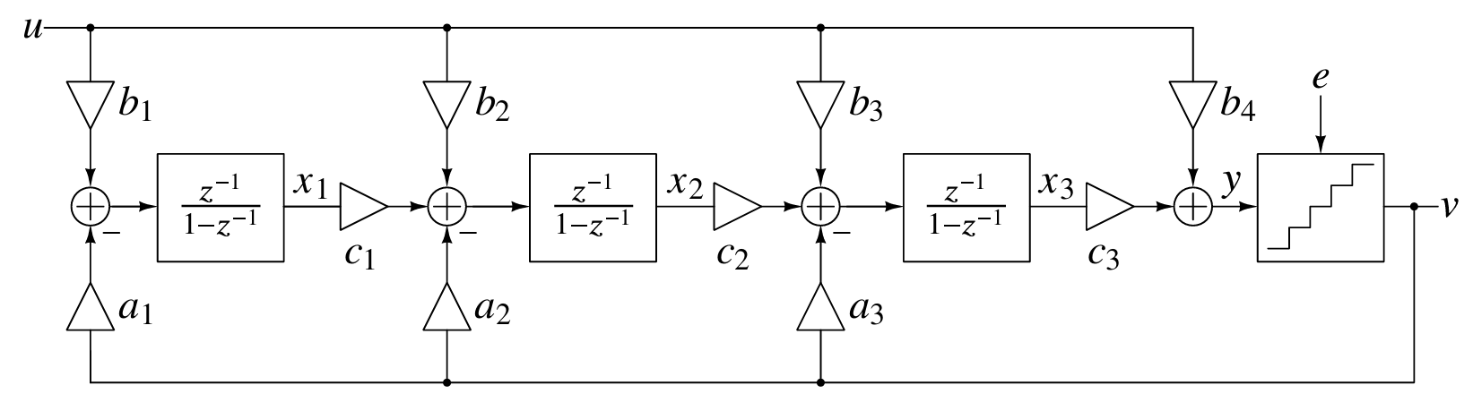
The example uses a model where the 2nd-order CIFB ("MOD2") topology produces an NTF which exhibits a double zero at DC: . The STF is determined by the path from the last integrator to the quantizer, which depends on the integrator’s timing (delaying or non-delaying) and the presence of any direct feed-forward term.
Loop equations and transfer functions
For a generic order modulator, let the output be , the input be , and the quantization error be . You can express a single-quantizer delta-sigma loop as:
where is the feedforward signal path and is the feedback (noise) path realized by the integrator chain and the distributed DAC feedback coefficients[3].
For a 2nd-order lowpass CIFB topology, the loop consists of two cascaded discrete-time integrator [4], with distributed DAC feedback . They return the quantizer output to the first and second integrator inputs, the realization yields an NTF with a double zero at :
(the canonical “MOD2” result). The STF depends on whether you include a direct input term at the quantizer input adder. When you remove the direct feed-forward path and the quantizer sees only the last integrator output, the in-band STF is approximately a pure delay, .
Stability Constraint: The Lee Bound ()
During NTF synthesis, you bound the maximum out of band gain of the NTF[3]:
to ensure practical stability with a binary quantizer (Lee’s rule). For 2nd order low-pass single-bit modulators, typical choices are ; is a widely used starting point. Larger pushes noise further out of band (stronger shaping) but reduces stability margin. Smaller is more conservative. The MATLAB function synthesizeSTF enforces this bound.
A quick closed-form SQNR estimate for order, OSR R, and a full-scale sinusoidal input is
which for shows the familiar 15 dB per octave improvement with OSR, assuming the Lee bound and the integrator states remain within limits. Here, is the quantizer resolution in bits. This expression and its derivation (Ardalan–Paulos/Schreier) are standard in delta-sigma design references.
Estimate Theoretical performance for single bit, 2nd-Order, OSR=512
You can estimate the theoretical performance for an ideal discrete-time ΔΣ modulator by assuming white quantization noise, no tones/limit cycles, perfect loop linearity, and no circuit non-idealities. These non-idealities include noise, jitter, finite OTA gain or GBW, excess loop delay, DAC mismatch, etc.
During NTF synthesis you enforce stability via the Lee bound . Under these assumptions, the peak in band quantization noise limited SQNR for an -order, single-bit quantizer modulator with oversampling ratio is well approximated by equation mentioned in Stability constraint (Lee Bound section). Putting it together for this case:
% Specs
Nbits = 1;      % quantizer bits (single-bit)
L = 2;      % modulator order
R = 512;    % oversampling ratio

% Solve
SQNR = 6.02*Nbits + 1.76 + (20*L + 10)*log10(R) ...
    - 10*log10( (pi^(2*L)) / (2*L + 1) );
ENOB = (SQNR - 1.76)/6.02;

fprintf('SQNR ≈ %.2f dB\nENOB ≈ %.2f bits', SQNR, ENOB);
SQNR ≈ 130.35 dB
ENOB ≈ 21.36 bits
Coefficient roles and SC mapping
In this example, you work with four sets of realization coefficients: b, a, c, and g. Each set defined how input and feedback signals enter the integrator chain[3].
Input feed-in coefficients : into the first summing node, into the second, and optional direct input to the quantizer input adder. In SC, are set by capacitor ratios of both integrators.
Distributed DAC feedback : from back into the first and second integrator inputs; in SC, when the same capacitor is reused for sampling vs. feedback or implemented via explicit feedback caps/switches.
Feedforward taps : feedforward taps to the quantizer input.
The local cross-feedback (resonator) : The value can be for a pure lowpass CIFB.
A representative CIFB structure with feedforward:
Robust behavioral to physical mapping for CIFB
Below is a clean, reproducible MATLAB snippet that follows the recommended flow, constrains the feedback to the SC ratios by a state similarity transform.
%% CIFB Flow with SC-aware 'a' Coefficient Matching
% This script designs a 2nd-order CIFB modulator, scales it for maximum
% stable amplitude, and then re-calculates coefficients to match physical
% switched-capacitor constraints.

% ---- 1. Specifications ----
order = 2;
osr   = 512;
opt   = 1;          % Use 1 for optimized NTF zeros
hInf  = 1.5;        % Lee criterion for stability (robustness)
arch  = 'CIFB';
nLev  = 2;          % Number of quantizer levels (2 for 1-bit)
xLim  = [1, 1];     % State limits for dynamic range scaling

% ---- 2. Synthesize NTF and Realize Initial Ideal Coefficients ----
ntf = synthesizeNTF(order, osr, opt, hInf);
[a, g, b, c] = realizeNTF(ntf, arch);

% ---- 3. Scale for Dynamic Range (Finds Maximum Stable Amplitude) ----
abcd = stuffABCD(a, g, b, c, arch);
[abcdScaled, uMax] = scaleABCD(abcd, nLev, 0, xLim);

% ---- 4. Define Physical Target and Find Optimal Scaling ----
% Define the target for the integrator gains 'a' based on physical Cs/Ci ratios.
aTarget = [0.5, 0.5];

% Set up the optimization to find the similarity transform scaling factors.
sInit = [1, 1]; % Initial guess for scaling factors [s1, s2]
opts = optimset('TolX', 1e-4, 'Display', 'off');

% Use fminsearch to find the optimal scaling factors 's' that make the
% resulting 'a' coefficients match aTarget.
sOpt = fminsearch(@(s) costFunction(s, abcdScaled, aTarget, arch), sInit, opts);

% ---- 5. Apply Optimal Scaling and Get Final, Realizable Coefficients ----
sOptMatrix = diag(sOpt);

% Apply the similarity transform: A'=S*A*inv(S), B'=S*B, C'=C*inv(S)
abcdFinal = [sOptMatrix * abcdScaled(1:order, 1:order) / sOptMatrix, sOptMatrix * abcdScaled(1:order, order+1:end); ...
    abcdScaled(order+1:end, 1:order) / sOptMatrix, abcdScaled(order+1:end, order+1:end)];

[aFinal, gFinal, bFinal, cFinal] = mapABCD(abcdFinal, arch);

% ---- 6. Report Final Coefficients ----
% Helper to format numeric vectors
fmtvec = @(v) strjoin(compose('%.4f', v), ' ');

% Single fprintf that prints all lines in one output block
fprintf(['Final CIFB Coefficients (SC-aware and Robust):\n' ...
    '  a = [%s] (Target: [%.2f %.2f])\n' ...
    '  g = [%s]\n' ...
    '  b = [%s]\n' ...
    '  c = [%s]\n' ...
    '\nMax Stable Input (MSA) is approx. uMax = %.3f (normalized amplitude)\n'], ...
    fmtvec(aFinal), aTarget(1), aTarget(2), ...
    fmtvec(gFinal), fmtvec(bFinal), fmtvec(cFinal), uMax);
Final CIFB Coefficients (SC-aware and Robust):
  a = [0.5000 0.5000] (Target: [0.50 0.50])
  g = [0.0000]
  b = [0.5000 0.5000 1.0000]
  c = [0.2792 1.5497]

Max Stable Input (MSA) is approx. uMax = 0.967 (normalized amplitude)
%% Helper function for fminsearch optimization
function err = costFunction(s, abcdMatrix, aTarget, arch)
% This function calculates the error between the current 'a'
% coefficients and the target 'a' for a given scaling vector 's'.

order = size(aTarget, 2);
sMatrix = diag(s);

% Apply the similarity transform to the state-space matrix
abcdTemp = [sMatrix * abcdMatrix(1:order, 1:order) / sMatrix, sMatrix * abcdMatrix(1:order, order+1:end); ...
    abcdMatrix(order+1:end, 1:order) / sMatrix, abcdMatrix(order+1:end, order+1:end)];

% Map back to coefficients to see the effect of our scaling
[aCurrent, ~, ~, ~] = mapABCD(abcdTemp, arch);

% Calculate the error (how far are we from our target?)
err = norm(aCurrent - aTarget);
end
This preserves NTF/STF (similarity transforms do not change I/O transfers) and gives you SC aware coefficients with non-zero c taps for feedforward shaping. These values are set directly into the model in respective Gain blocks.
Component Sizing & Operating Point for SC CIFB
Next step in the design process begins with selecting capacitors’ sizes and OTA specifications that satisfy three practical constraints: (1) the integrator gain is in the practical 0.4–0.7 window range for symmetry and tolerance to the typical SC non‑idealities, (2) The thermal noise remains low, and (3) The OTA settling/slew within a half clock phase is comfortably met for 10.24 MHz SC loop (ADS1209 nominal modulator rate is 10 MHz; example uses 10.24 MHz so that OSR = 512 gives a 20 kHz baseband and power‑of‑two decimation).
Capacitor Sizing
First integrator
(integration capacitor)
(sampling capacitor)
Gain:
Second integrator
Gain:
Load at the output node(s)
(routing, sampler, stray/MIM bottom-plate budget)
The second integrator uses capacitors scaled down by 2× because signal swing at this node is attenuated by the first stage, allowing area savings while maintaining noise performance. Both stages use b = 0.5, which provides an optimal trade-off between loop gain (for noise shaping) and sensitivity to parasitics. With , the SC integrator transfer is:
which hits the sweet spot: enough loop gain to support strong noise shaping, yet modest capacitor sizes for area, matching, and parasitic tolerance. Keeping and in the low range yields benign and manageable switch bottom‑plate feedthrough and effects in a 10–20 MHz clock regime.
Thermal Noise Check
You can estimate the thermal noise at 300K using:
For
For
Thermal noise from the first sampling capacitor is not shaped by the NTF - it appears directly as input-referred noise. Following the standard SC noise model, the switch contributes a single‑sided noise spectral density , and the foldover of this noise during sampling produces a sampled noise spectrum approximately equal to [4]. Integrating this spectrum over the signal band yields an in‑band thermal noise power consistent with the familiar scaling. You can conservatively estimate the in-band thermal noise power after decimation for simplified analysis as:
For a signal (), the input RMS is approximately . The thermal-noise-limited SNR is:
Since the coarse quantization yields an SQNR typically in the 100–105 dB range for a second-order loop at OSR = 512, the quantization noise will dominate the total SNR, confirming that thermal noise is not the design bottleneck.
OTA Operating Points
You can set the OTA operating points as:
The OTA DC gain gives negligible static error in charge transfer. Practical designs often target 60–80 dB for low-pass SC loops, so (~80 dB) is conservative. The output swing parameter follows the specification of the reference device used for this example.
For a single-pole OTA with load , you can estimate settling time:
Time constant:
settling (14-bit accuracy): ≈ 1.9 ns
Available half-phase for sampling at 10.24 MHz: 48.8 ns
Note: Although for the chosen capacitance values at 10.24MHz, you can further reduce these values to: . They still satisfy single-phase settling and provide ample slew margin. For the chosen values in example, the performance is saturated with minimal over-provisioning.
Decimation Filter Architecture
You can implement a computationally efficient decimation chain for high OSR ADCs using a multistage cascade. The idea is to perform most of the rate reduction with multiplier free CIC filters[3]. You then equalize their passband droop at a lower rate, and finally apply a halfband FIR to finish the decimation with a sharp transition band. This partitioning maximizes hardware efficiency at very high input rates while preserving in-band fidelity.
Architecture: [CIC Chain] → [Compensation FIR] → [Halfband FIR]
CIC Filter Chain: bulk decimation using Cascaded Integrator–Comb filters - no multipliers, tiny memory; the tradeoff is significant passband droop and a wide transition region.
Compensation FIR (COMP): equalizes the CIC droop at a lower intermediate rate; designed to approximate the inverse of the composite CIC passband magnitude.
Halfband FIR: final decimate-by-2 with linear phase; ~50% of coefficients are zero and passband/stopband ripples are equal - ideal for efficient implementations.
This cascade is standard practice in multirate DSP and in oversampled Delta-Sigma pipelines. It offers an excellent balance of filtering performance, hardware economy, and scalability[5].
You choose the CIC chain by decomposing the total decimation factor into a sequence of R=2 stages and selecting the order (number of integrator–comb pairs) per stage to meet an overall alias attenuation target. Hogenauer’s formulation shows the CIC transfer as:
with is the stage decimation ratio, is the differential delay, and the number of cascaded sections. In practice, you treat the CIC magnitude as a product of sinc terms and assign larger orders at lower rate stages where computation is cheaper. You can use the following MATLAB code to generate the CIC chain:
% ---------- Initial Setup ----------
OSR_total = 512;
N = 2; % Decimation factor for each stage
attenTargetdB = 100;

% Last stage is FIR halfband → CIC stages = log2(OSR_total)-1
numStages = log2(OSR_total) - 1;
% ---------- Per-stage calculations ----------
Stage       = (1:numStages).';
OSR_i       = OSR_total ./ (2.^Stage);
fp          = 1./(2*OSR_i);
fi          = 1 - 1./(2*OSR_i);
A1          = abs((sin(pi*fp).*sin(pi*fi/N)) ./ (sin(pi*fp/N).*sin(pi*fi)));
A1_dB       = 20*log10(A1);
SincOrder   = ceil(attenTargetdB ./ A1_dB);

% Correct droop calculation (normalized to DC gain)
Droop_dB    = zeros(numStages,1);
for i = 1:numStages
    H_fp_i = abs((sin(pi*N*fp(i)) / sin(pi*fp(i)))^SincOrder(i));
    Droop_dB(i) = 20*log10(H_fp_i / (N^SincOrder(i))); % normalized droop- need to check calculation
end

T = table(Stage, OSR_i, fp, fi, A1, A1_dB, SincOrder, ...
    'VariableNames', {'Stage','OSR_i','f_p','f_i','A1','A1_dB','sincOrder'});

header   = 'Tabular results for decimate-by-2 CIC stages:';
tblTxt = evalc('disp(T)');
fprintf('%s\n%s', header, tblTxt);
Tabular results for decimate-by-2 CIC stages:
    Stage    OSR_i       f_p         f_i        A1      A1_dB     sincOrder
    _____    _____    _________    _______    ______    ______    _________

      1       256     0.0019531    0.99805    325.95    50.263        2
      2       128     0.0039062    0.99609    162.97    44.242        3
      3        64     0.0078125    0.99219    81.483    38.221        3
      4        32      0.015625    0.98438    40.735    32.199        4
      5        16       0.03125    0.96875    20.355    26.174        4
      6         8        0.0625     0.9375    10.153    20.132        5
      7         4         0.125      0.875    5.0273    14.027        8
      8         2          0.25       0.75    2.4142    7.6555       14
Tabular results for decimate-by-2 CIC stages (Total OSR=256, target attenuation ~100 dB) is displayed above.
Here, denotes the stage passband edge normalized to that stage’s rate, the worst-case alias location, the first-order attenuation, and the computed order.
As the rate drops, higher-order CIC sections become very cheap per sample; pushing the most selective filtering to the slowest stages is both efficient and effective. To compute the coefficients of compensation filter, you can use the following MATLAB code:
%----------- Compensator Design -----------
SincOrder = flipud(SincOrder)';
compOrder = 8;
fp = 0.25;
numStages    = numel(SincOrder);
expectedOsr  = 2^numStages;      % CIC portion (without halfband)
if OSR_total/2 ~= expectedOsr
    warning('OSR=%d but %d stages give %d:1. Adjust stages or OSR.', ...
        osr*2, numStages, expectedOsr);
end

% Design grid (folded axis; 1 == Nyquist at final rate)
npb = 20;
f   = linspace(0, fp, 2*npb);
% Composite CIC/sinc magnitude using zinc
H = ones(size(f));
for i = 1:numStages
    H = H .* zinc(f / (2^i), 2, SincOrder(i));   % n=2 stage, order=orders(i)
end
% Parks–McClellan design to invert the composite CIC droop
wt = abs(H(1:2:end));
b  = firpm(compOrder, 2*f, 1./max(abs(H), eps), wt);

%----------- Report Results -----------
orderStr = strjoin(string(SincOrder(:).'), ' ');
coeffStr = strtrim(sprintf('%.4f ', b));

fprintf(['\nOverall CIC + Compensator Design\n' ...
    '  OSR: %d:1 (%d stages)\n' ...
    '  CIC orders: [%s]\n' ...
    '  Compensator taps: %d\n' ...
    '  Coefficients: [%s]\n'], ...
    expectedOsr, numStages, orderStr, compOrder+1, coeffStr);
Overall CIC + Compensator Design
  OSR: 256:1 (8 stages)
  CIC orders: [14 8 5 4 4 3 3 2]
  Compensator taps: 9
  Coefficients: [0.0709 -0.4967 1.8362 -4.4977 7.1755 -4.4977 1.8362 -0.4967 0.0709]
For orders computed in previous section, the coefficients of 8 tap COMP FIR are displayed above.
Design of the Halfband FIR Filter
You use the halfband FIR to perform the final decimate-by-2 and to supply a sharp transition band to meet overall stopband attenuation. Halfband FIRs have three key properties: (i) symmetry around (normalized), (ii) ~50% coefficients exactly zero (every other tap), and (iii) linear phase - making them both efficient and phase-transparent. They are typically designed via equiripple methods.
Design intent: You target the following specifications:
StopbandAttenuation:
TransitionWidth: (from passband edge to stopband start at 0.55 in normalized Nyquist-units)
Method: "equiripple"
Using designHalfbandFIR function with the above targets yields a linear phase halfband whose alternating coefficients are zero, enabling an efficient polyphase decimator-by-2.
designHalfbandFIR(...
StopbandAttenuation=-db(1e-5),...
TransitionWidth=2*(0.5-0.45),...
DesignMethod="equiripple");
Passband/stopband ripples are equal by construction, and symmetry about holds.

Final DSM model & ADS1209 Benchmark
The model is attached in the example as 'SCbasedSecondOrderDSM.slx'. You can load the block parameters by running the following script:
modelParamsSCDSM;
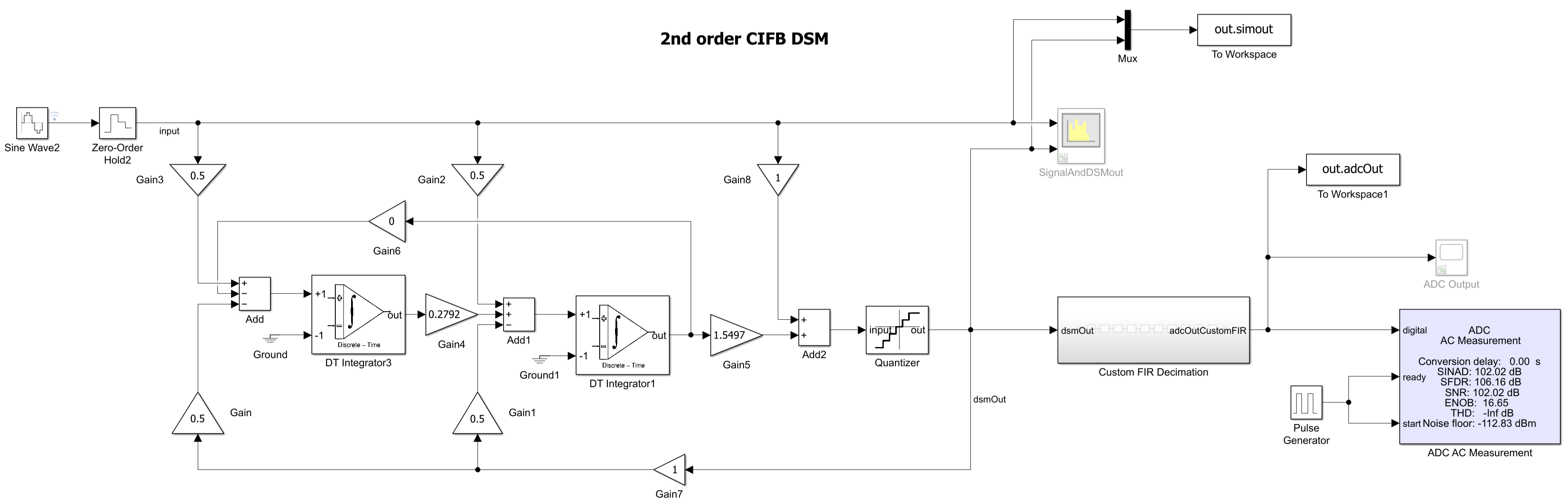
The ADC AC measurement block in the example reports:
SINAD/SNR = 102.02 dB
SFDR = 106.16 dB
ENOB = 16.65 bits
Noise floor = -112.83 dBm
The simulated model here shows an SNR improvement of approximately 2–10 dB over the typical AC performance values reported for the ADS1209. This is expected because the model operates at a system‑level abstraction, where the focus is on architectural behavior and the dominant circuit‑impairment mechanisms, rather than on detailed device‑level effects.
At this abstraction level, the SC integrators include the primary non‑idealities relevant to loop dynamics—such as finite gain, integration error, thermal noise contribution, and coefficient mismatches—but they do not attempt to reproduce every physical mechanism present in silicon. Effects such as board‑level parasitics, package coupling, reference network imperfections, input‑stage loading, and layout‑dependent noise mechanisms are handled later in the design flow using transistor‑level tools. This behavioral abstraction is particularly well‑suited for design‑space exploration, architectural tradeoff analysis, and early‑stage performance evaluation, providing fast and numerically stable simulations without the convergence challenges and computational cost associated with device‑level models[4].
For context, the corresponding theoretical upper bound for an ideal second‑order DSM with the same OSR gave SQNR 130.35 dB and ENOB 21.36 bits, which represents the performance of a perfectly linear loop with ideal quantization noise shaping. The gap between the theoretical limit, the system‑level simulation results, and the measured silicon performance illustrates how constraints accumulate as the design progresses from ideal theory to behavioral models and finally to circuit‑level realization.
© Copyright 2025 The MathWorks, Inc.
References
[1] ADS1209 Data Sheet, Product Information and Support | TI.Com. Accessed January 29, 2026. https://www.ti.com/product/ADS1209.
[2] Kuo, B. C. Digital Control Systems. Holt, Rinehart and Winston, 1980.
[3] Pavan, Shanthi, Richard Schreier, and Gabor C. Temes. Understanding Delta-Sigma Data Converters. John Wiley & Sons, 2017.
[4] De La Rosa, José M. Sigma‐Delta Converters: Practical Design Guide. 2nd ed. Wiley, 2022.
[5] Hogenauer, E. An Economical Class of Digital Filters for Decimation and Interpolation. IEEE Transactions on Acoustics, Speech, and Signal Processing 29, no. 2 (1981): 155–62. https://doi.org/10.1109/TASSP.1981.1163535.