Main Content

MOSFET (Ideal, Switching)

R2026b

Ideal N-channel MOSFET for switching applications

  • MOSFET (Ideal, Switching) block

Libraries:
Simscape / Electrical / Semiconductors & Converters

Description

The MOSFET (Ideal, Switching) block models the ideal switching behavior of an n-channel metal-oxide-semiconductor field-effect transistor (MOSFET).

The switching characteristic of an n-channel MOSFET is such that if the gate-source voltage exceeds the specified threshold voltage, the MOSFET is in the on state. Otherwise, the device is in the off state. This figure shows a typical i-v characteristic:
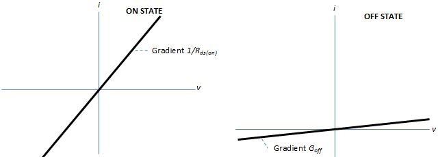
Graphs showing linear i-v characteristics. In the on state, the slope is the reciprocal of the on-state resistance. In the off state, the slope is the off-state conductance.

To define the I-V characteristic of the MOSFET, set the On-state behavior and switching losses parameter to either Specify constant values or Tabulate. The Tabulate option is available only if you expose the thermal port of the block.

In the on state, the drain-source path behaves like a linear resistor with resistance, Rds_on. However, if you expose the thermal port of the block and parameterize the device using tabulated I-V data, the tabulated resistance is a function of the temperature and current.

In the off state, the drain-source path behaves like a linear resistor with low off-state conductance, Goff.

Then, the defining Simscape™ equations for the block are:

    if G > Vth       v == i*Rds_on;     else       v == i/Goff;     end 

where:

  • G depends on the value of the Gate-control port parameter.

    • If you set the Gate-control port parameter to PS, you control the gate terminal through a physical signal. G is the value at the input port G.

    • If you set the Gate-control port parameter to Electrical, you control the gate terminal through an electrical signal. G is equal to:

          if v >= 0        G = G.v - S.v;     else       G = G.v - D.v;     end 

      where G.v is the gate voltage, S.v is the source voltage, and D.v is the drain voltage.

  • Vth is the threshold voltage.

  • v is the drain-source voltage.

  • i is the drain-source current.

  • Rds_on is the on-state resistance.

  • Goff is the off-state conductance.

Using the Integral Diode settings, you can include the body diode or an integral protection diode. The integral diode provides a conduction path for reverse current and allows for an increased numerical stability in your model. For example, to provide a path for a high reverse-voltage spike that is generated when a semiconductor device suddenly switches off the voltage supply to an inductive load.

Model Gate Port and Thermal Effects

You can choose between physical or electrical ports to control the gate terminal and expose the thermal port to model the heat that switching events and conduction losses generate. To choose the gate-control port, set the Gate-control port parameter to PS or Electrical. To expose the thermal port, set the Modeling option parameter to No thermal port or Show thermal port.

You can also expose the thermal port HDiode of the integral protection diode by selecting the Separate thermal port for integral diode parameter. If you do not expose the diode thermal port, both the device and the diode share the common thermal port, H. (since R2024b)

For more information about using thermal ports, see Simulating Thermal Effects in Semiconductors.

Thermal Losses

The MOSFET (Ideal, Switching) block models three types of thermal losses: conduction losses, switching losses, and reverse recovery losses of the integral diode.

Conduction Losses

The block calculates conduction losses as the instantaneous electrical power dissipated by the device, P = iv, using either a fixed on‑state resistance or a temperature‑dependent on‑state voltage characteristic. The block draws the requisite electrical power from the supply in through the ports and converts it to thermal power. If you set the Modeling option parameter to No thermal port, the block dissipates this thermal power to the external system. If you set the Modeling option parameter to Show thermal port, the block continuously injects this power into the thermal network as heat.

The power_dissipated variable in the logged simulation data reports ohmic on-state losses. This variable does not include switching losses or reverse recovery losses because the block models these losses as instantaneous events.

Switching Losses

Switching losses are major sources of thermal loss in semiconductors. During each on-off switching transition, the MOSFET parasitics store and then dissipate energy. To model switching losses, set the Modeling option parameter to Show thermal port. The MOSFET (Ideal, Switching) block uses an abstract model that simulates fast and does not model charge dynamics. The model treats switching losses as discrete energy packets that occur at switching events, instead of continuous power.

The figure shows an idealized representation of the output voltage Vout and current Iout of the semiconductor device. The interval includes the nth switching cycle, during which the device turns on and then off.
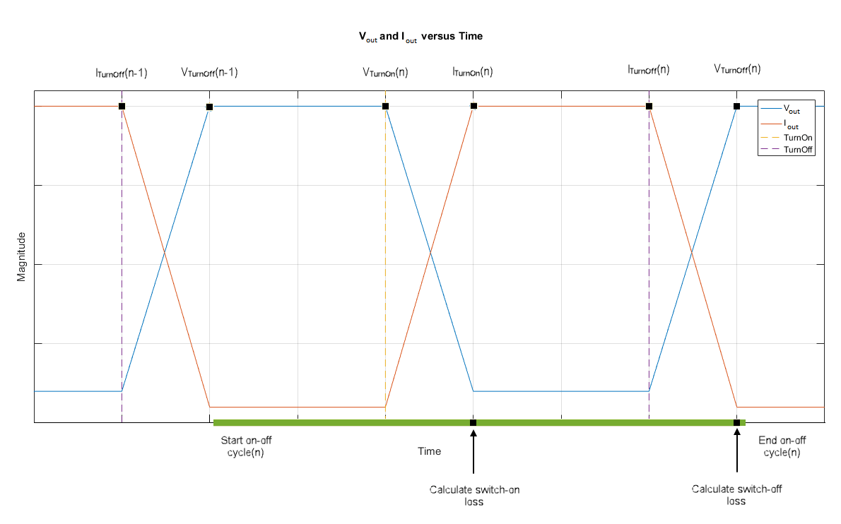
Figure showing changes in current and voltage over a switching cycle. At the start of the cycle, current and voltage are at steady off-state values. At turn on, current ramps up linearly and voltage ramps down linearly to their steady on-state values. At turn off, current ramps down linearly and voltage ramps up linearly back to their steady off-state values.

When a switching device turns on, the loss depends on the off-state voltage across the device just prior to turn on and the on-state current when the device reaches its fully on state. Similarly, when a switching device turns off, the loss depends on the on-state current through the device just prior turn off and the off-state voltage across it when it reaches its fully off state.

To compute the switching losses, you specify the energy dissipated during a single switch-on and switch-off event. You also specify the corresponding reference values of off-state voltage and on-state current at which you quote the losses. Choose how to parameterize the losses depending on the data you have.

  • To specify a scalar value for the switching losses, set the On-state behavior and switching losses parameter to Specify constant values. The Switch-on loss and Switch-off loss parameter values set the sizes of the switching losses. The block scales the losses by the measured off-state voltage and the on-state current.

  • To specify the losses as a function of the junction temperature and on-state current at a fixed off-state voltage, set the On-state behavior and switching losses parameter to Tabulate and clear the Include switching loss tabulation with off-state Vds voltage parameter. The Switch-on loss, Eon(Tj,Ids) and Switch-off, Eoff(Tj,Ids) parameters set the size of the losses. The block scales the losses measured by the off-state voltage.

  • To specify the losses as a function of the junction temperature, on-state current, and off-state voltage, set the On-state behavior and switching losses parameter to Tabulate and select the Include switching loss tabulation with off-state Vds voltage parameter.

You can choose when to take some of the measurements that the block uses to calculate switching losses. Some circuits deviate from the idealized case shown in the figure. For example, there can be transient peaks in current during turn on due to output capacitance or transient peaks in voltage during turn off due to parasitic inductance. Manufacturers quote losses at the voltage and current values after any transients due to parasitics, hereafter referred to as steady-state values.

The off-state voltage at turn on is always steady so to calculate Eon the block measures the voltage at turn on VTurnOn. You can choose when to measure the on-state current:

  • If the current is not steady immediately after turn on and the final on-state value does not vary between consecutive cycles, use the final on-state value from the previous cycle ITurnOff(n-1). (since R2023b)

  • If the current is steady immediately after turn on, use the initial on-state current from the present cycle ITurnOn(n).

  • If the current is not steady immediately after turn on and the on-state value varies between consecutive cycles, specify a delay following turn on before the block measures the current ITurnOn(n) < Iout(n) < ITurnOff(n). (since R2026b)

Similarly, to calculate Eoff the block measures the on-state current at turn off ITurnOff(n). You can choose when to measure the off-state voltage to avoid transients:

  • At the end of the last off period VTurnOn(n)

  • At the start of the present cycle VTurnOff(n)

  • Following turn off after a short delay VTurnOff(n) < Vout (n)< VTurnOn(n+1)

For conventional switched-mode power supplies, using measurements from the previous cycle is the most robust option because switching transients do not affect the measured values. To take measurements from the previous cycle, select the Use last on-state current from previous cycle for turn-on loss and Use last off-state voltage from previous cycle for turn-off loss parameters. You also need to take one of the current or voltage measurements from the previous cycle if:

  • You are modeling a capacitance across the switching device, for example, if the protection diode has capacitance or you are using the Lauritzen charge model. The capacitance causes a current overshoot at turn-on, so ITurnOn(n) does not represent the steady-state value. The best practice is not to model capacitance across the switching device, because this mixes an abstracted model for the switching device with a detailed physics model for the diode. If you must model capacitance across the switching device, you can use the current measurement at the end of the last on-period ITurnOff(n-1) to calculate Eon. To enable this option, select the Use last on-state current from previous cycle for turn-on loss parameter.

  • You are modeling switching device lead inductance. The inductance causes a voltage overshoot at turn off, so VTurnOff(n) does not represent the steady-state value. The best practice is not to model switching device lead inductance, because the time constant associated with lead inductance is typically much smaller than the pulse-width modulation (PWM) period. This smaller time constant means that the simulation requires smaller simulation time steps, slowing down the simulation. If you must model switching device lead inductance, select the Use last off-state voltage from previous cycle for turn-off loss parameter to use the voltage measurement at the end of the last off period, VTurnOn(n) to calculate Eoff.

Resonant converters switch when there are no losses using zero-current or zero-voltage switching (ZCS or ZVS). A converter design might achieve ZCS and ZVS only at particular operating points, or achieve only one of ZCS and ZVS. Because the operating point, for example device current, can vary so much between turn on and turn off, you sometimes need to make the measurements of current or voltage at the switching event. To calculate turn-on loss using the initial on-state current measurement immediately after turn on, clear the Use last on-state current from previous cycle for turn-on loss parameter and set the On-state current measurement delay parameter to 0. To calculate turn-off loss using the initial off-state voltage measurement immediately after turn off, clear the Use last off-state voltage from previous cycle for turn-off loss parameter and set the Off-state voltage measurement delay parameter to 0.

When making measurements at the switching event, transient dynamics in the off-state voltage or on-state current can result in an incorrect measurement value. Wait for any transients to settle down before taking the measurement. If your circuit has a current overshoot before the on-state current reaches a steady state, then set the On-state current measurement delay parameter to a value that is slightly longer than the current overshoot time. If your circuit has a voltage transient before the off-state voltage reaches a steady state, then set the Off-state voltage measurement delay parameter to a value that is slightly longer than the transient.

Examine the simulation results to check that the current and voltage behave as you expect. The ziOff variable in the logged simulation data represents the current at turn off and ziOn represents the current measured after turn‑on including any delay. Similarly, zvOn represents the voltage at turn on and zvOff represents the voltage measured after turn on including any delay. Use these variables to verify that the sampled current and voltage values are at steady state and representative of the intended operating point. To learn how to log and plot simulation data, see the Log and Plot Simulation Data example.

This table summarizes when to measure the on-state current to accurately calculate Eon for common power electronics applications. The block measures the voltage at turn on VTurnOn(n).

Currents Measurements for Calculating Turn-on Losses

ApplicationsCurrent MeasurementParameter ValuesVariable in Logged Simulation Data
  • Conventional PWM converters

  • Circuits with output capacitance causing turn‑on current spikes

The final value of the on‑state current at the end of the last on period, measured at turn off ITurnOff(n-1)
  • Select the Use last on-state current from previous cycle for turn-on loss parameter.

ziOff
  • Resonant converters with effective ZCS at turn‑on

  • Operating points where turn‑on current defines loss

The initial on-state current from the present cycle, measured just after turn on ITurnOn(n)
  • Clear the Use last on-state current from previous cycle for turn-on loss parameter

  • Set the On-state current measurement delay parameter to zero.

ziOn
  • Circuits with brief capacitive current overshoot

  • Quasi‑resonant converters that are not perfectly ZCS

The on-state current during the present cycle, measured a short delay after turn on ITurnOn(n) < Iout(n) < ITurnOff(n)
  • Clear the Use last on-state current from previous cycle for turn-on loss parameter

  • Set the On-state current measurement delay parameter to a value that is slightly longer than the current overshoot time.

ziOn

This table summarizes when to measure the off-state voltage to accurately calculate Eoff for common power electronics applications. The block measures the current at turn on ITurnOff(n).

Voltage Measurements for Calculating Turn-off Losses

ApplicationsVoltage MeasurementParameter ValuesVariable in Logged Simulation Data
  • Conventional PWM converters

  • Circuits with parasitic inductance causing turn‑off overshoot

The final value of the off‑state voltage at the end of the last off period, measured at turn on VTurnOn(n)
  • Select the Use last off-state voltage from previous cycle for turn-off loss parameter.

zvOn
  • Resonant converters with effective ZVS at turn‑off

  • Operating points where turn‑on voltage defines loss

The initial off-state voltage from the present cycle, measured just after turn off VTurnOff(n)
  • Clear the Use last off-state voltage from previous cycle for turn-off loss parameter

  • Set the Off-state voltage measurement delay parameter to zero.

zvOff
  • Circuits with short voltage transients due to stray inductance

  • Quasi‑resonant converters that are not perfectly ZVS

The off-state voltage during the present cycle, measured a short delay after turn off VTurnOff(n) < Vout (n) < VTurnOn(n+1)
  • Clear the Use last off-state voltage from previous cycle for turn-off loss parameter

  • Set the Off-state voltage measurement delay parameter to a value that is slightly longer than the voltage transient.

zvOff

The MOSFET (Ideal, Switching) block applies switching losses to the thermal port by stepping up the junction temperature, at switching events, with a value equal to the switching loss divided by the total thermal mass at the junction. However, the blocks does not draw an equivalent amount of energy from the power supply. The block is unable to draw this electrical energy from the electrical ports because drawing the energy requires a power source that is always connected to the switching device. In a switching converter, the switching device only sees the power source for a subset of the switching cycle so it is not possible to draw this electrical energy from the supply instantaneously at each switching event. The block effectively draws this electrical energy in from outside the electrical and thermal networks, in order to have the correct thermal energy balance. If your circuit has a half-bridge structure, you can use Half-Bridge (Ideal, Switching) block, which can draw equivalent energy from the supply, instead. If you need to use the MOSFET (Ideal, Switching) block, you can draw equivalent energy from the supply using a Probe block. For more information, see the Apply IGBT Switching Losses to Electrical Supply example.

Reverse Recovery Losses

Reverse recovery loss can be a significant source of thermal loss in diodes. The diode dissipates energy every time it turns off, from its conducting state to the open-circuit state. To model reverse recovery loss:

  • Set Modeling option to Show thermal port.

  • Set Integral protection diode to Diode with no dynamics.

If you set the Reverse recovery loss model parameter to Tabulate loss with Tj and If, the value of the Reverse recovery loss table, Erec(Tj, If) parameter specifies the dissipated energy as a function of the junction temperature and the forward current just before the switching event. The off-state voltage linearly scales the losses relative to the Turn-off voltage when measuring recovery loss, Vrec parameter value. The table uses delayed values for the current and voltage. To use a value in the lookup table that is close to the instantaneous value, set the Filter time constant for voltage and current values parameter to a value that is lower than the fastest switching period.

If you set the Reverse recovery loss model parameter to Tabulate loss with Tj, If, and Vrec, the value of the Reverse recovery loss table, Erec(Tj, If, Vrec) parameter specifies the dissipated energy as a function of the junction temperature, forward current just before the switching event, and off-state voltage after the reverse recovery event. The table uses delayed values for the current and voltage. To use a value in the lookup table that is close to the instantaneous value, set the Filter time constant for voltage and current values parameter to a value that is lower than the fastest switching period. (since R2026a)

If you set the Reverse recovery loss model parameter to Fixed loss, the value of the Reverse recovery loss parameter specifies the energy dissipated during each turn-off event. If you select the Scale reverse recovery loss with current and voltage parameter, then the block scales this loss value linearly by the on-state current and the off-state voltage. To use scaling values that are close to the instantaneous values, set Filter time constant for voltage and current values to a value that is lower than the fastest switching period.

Parameterization

The MOSFET (Ideal, Switching) block supports multiple predefined parameterizations.

Use this parameterization data to represent components by specific suppliers. The parameterizations of these MOSFETs match the manufacturer data sheets. To load a predefined parameterization, double-click the MOSFET (Ideal, Switching) block, click the <click to select> hyperlink of the Selected part parameter, and, in the Block Parameterization Manager window, select the part you want to use from the list of available components.

Note

The predefined parameterizations of Simscape components use available data sources for the parameter values. Engineering judgment and simplifying assumptions are used to fill in for missing data. As a result, expect deviations between simulated and actual physical behavior. To ensure accuracy, validate the simulated behavior against experimental data and refine component models as necessary.

For more information about predefined parameterization and a list of the available components, see Simscape Electrical Part Collection.

You can also use the ee_importDeviceParameters function to extract the device parameters from an XML file and import them into the block. The XML file must be on the MATLAB® path and must use a parameterization format supported by Hitachi.

Variables

To set the priority and initial target values for the block variables before simulation, use the Initial Targets section in the block dialog box or Property Inspector. For more information, see Set Priority and Initial Target for Block Variables.

Use nominal values to specify the expected magnitude of a variable in a model. Using system scaling based on nominal values increases the simulation robustness. Nominal values can come from different sources. One of these sources is the Nominal Values section in the block dialog box or Property Inspector. For more information, see System Scaling by Nominal Values.

Generate Derived Data Sheet

Since R2026a

You can generate a derived data sheet for the MOSFET (Ideal, Switching) block that contains summary tables and characteristic plots similar to those that device manufacturers provide in their data sheets. A built-in MATLAB script calculates the block-level characteristics based on the parameter values in your model. Use derived data sheets to explore the effect of your parameter choices on device characteristics, help you select manufactured parts, or share your component-level design with others.

The derived data sheet for the MOSFET (Ideal, Switching) block includes these plots:

  • Drain current versus drain-source voltage at different temperatures

  • Switch-on loss and switch-off loss versus drain current at different temperatures

  • Surface plots of switching losses, with respect to the on-state current and off-state voltage, at different temperatures

  • Surface plot of switching losses, with respect to on-state current and junction temperature, at maximum off-state voltage

  • Forward voltage versus current of the body diode at different temperatures

  • Reverse recovery loss versus diode current (since R2026b)

  • Surface plots of the reverse recovery loss, as a function of the on-state current and off-state voltage, at different temperatures (since R2026b)

  • Surface plot of the reverse recovery loss, as a function of the on-state current and junction temperature, at the maximum off-state voltage (since R2026b)

  • Off-state drain current voltage versus off-state drain-source voltage

  • Off-state forward voltage versus current of the body diode

To generate a derived data sheet:

  1. Open the MATLAB script by clicking the Open live script button next to the Derived data sheet parameter in the Utilities section of the block dialog box.

  2. Click the Generate Data Sheet button in the script.

For more information about derived data sheets, see Generate Derived Data Sheets.

Plot Basic I-V Characteristics

Since R2023b

You can plot the basic I-V characteristics of the MOSFET (Ideal, Switching) block without building a complete model. Use the plots to explore the impact of your parameter choices on device characteristics. If you parameterize the block from a data sheet, you can compare your plots to the data sheet to check that you parameterized the block correctly. If you have a complete working model but do not know which manufactured part to use, you can compare your plots to data sheets to help you decide.

To plot the basic characteristics, click the Plot button next to the Basic characteristics parameter. (since R2026a)

The Basic characteristics parameter generates different plots depending on the values you specify for the Modeling option, On-state behavior and switching losses, and Integral protection diode parameters of the MOSFET (Ideal, Switching) block. If you model the switching device with an integral protection diode, the Basic characteristics parameter plots the I-V characteristics for both the switching device and the diode. If you enable the thermal port of the block, the Basic characteristics parameter also generates surface plots of the turn-on energy loss and turn-off energy loss as functions of the on-state current and off-state voltage. For more information about this parameter, see Plot Basic I-V Characteristics of Semiconductor Blocks.

Examples
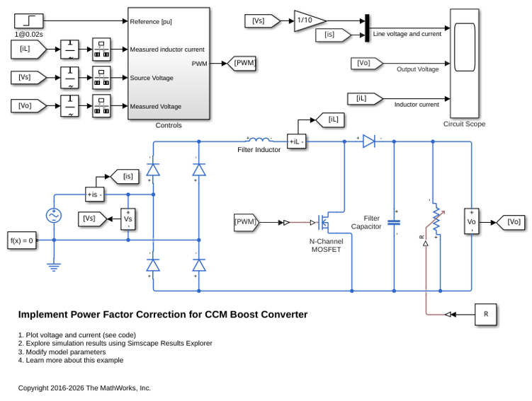
Assumptions and Limitations

  • The logged simulation data reports the thermal losses as lastTurnOffLoss, lastTurnOnLoss, and lastReverseRecoveryLoss. These variables record losses as a pulse with an amplitude equal to the energy loss. If you use a script to sum the total losses over a defined simulation period, you must sum the pulse values at each pulse rising edge. You can also access the total accumulated switching losses from the accumulatedSwitchingLosses variable in the logged simulation data. This variable sums all switching losses to date, including reverse recovery losses for the diode. Alternatively, you can extract conduction and switching losses from logged data using the ee_getPowerLossSummary and ee_getPowerLossTimeSeries functions.

  • If you are using a fixed-step solver, the shortest pulse on or pulse off that captures both the turn-on and turn-off losses is three time steps long. A turn-on pulse with length equal to the fixed step only reports turn-off losses. A turn-off pulse with length equal to the fixed step only reports turn-on losses.

  • If you operate the MOSFET in the reverse region (negative drain-source currents), the logged simulation data does not report any switch-on or switch-off losses because the parallel diode provides continuous parallel conduction. In the logged simulation data, ziOn reports zero current to implement the zero losses even if the current steps to a negative value.

  • If you select the On-state current measurement delay or the Off-state voltage measurement delay parameters in a fixed-step simulation, the step size must be small enough to give the requisite time resolution to make the measurement.

  • If you use tabulated data to model switching losses or reverse recovery losses, check that the temperature, current, and voltage are in the range you specify. If you do not define a realistic thermal model, for example, if the junction mass or the conductance from the junction to the case is too small, the temperature can exceed the range you specify, causing the block to extrapolate the losses to nonphysical values.

  • The MOSFET (Ideal, Switching) block does not support energy accounting. If you try to get energy information for this block using the getEnergyInfo function, the function generates an error message.

Ports

The figure shows the block port names.
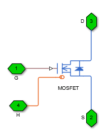
Figure showing the block icon with port names labeled. The gate terminal, G, and thermal port, H, are on the left. The drain terminal, D, and source terminal, S, are on the right.

Conserving

expand all

Port associated with the gate terminal. You can set the port to either a physical signal or electrical port.

Electrical conserving port associated with the source terminal.

Electrical conserving port associated with the drain terminal.

Thermal conserving port.

Dependencies

To enable this port, set Modeling option to Show thermal port.

Since R2024b

Thermal conserving port associated with the integral protection diode.

Dependencies

To enable this port, select the Separate thermal port for integral diode parameter.

Parameters

expand all

Whether to enable the thermal port.

Part Repository

Use the Select part button to open the Block Parameterization Manager tool and view the available parts.

Active part associated with the block.

Dependencies

To enable this parameter, apply a part to the block by using the Block Parameterization Manager.

Click the Restore parameters button to restore the parameterization to the active part. The name of the parameter is Status: unmodified if the part uses the default properties for the parameter, and Status: modified if the parameters have been modified from the associated active part.

Dependencies

To enable this parameter, apply a part to the block by using the Block Parameterization Manager.

Use the Clear part association button to clear the active part associated with the block.

Dependencies

To enable this parameter, apply a part to the block by using the Block Parameterization Manager.

Main

This table shows how the visibility of Main parameters depends on how you configure the Modeling option and On-state behavior and switching losses parameters. To learn how to read this table, see Parameter Dependencies.

Main Parameter Dependencies

Parameters and Options
Modeling option
No thermal portShow thermal port
Gate-control portGate-control port
Drain-source on resistance, R_DS(on)Threshold voltage, Vth
Off-state conductanceOn-state behavior and switching losses
Specify constant valuesTabulate
Threshold voltage, VthDrain-source on resistance, R_DS(on)On-state voltage, Vds(Tj,Ids)
Off-state conductanceTemperature vector, Tj
Drain-source current vector, Ids
Off-state conductance

Option to specify physical or electrical control port for the switch gate.

Note

If you set this parameter to Electrical, use an internal or external reverse diode along with this block. For numerical considerations, the forward voltage of the diode must be smaller than the value of the Threshold voltage, Vth parameter of this block.

Parameterization method for on-state behavior and switching losses, specified as one of these values:

  • Specify constant values — Use scalar values to specify the output current, switch-on loss, and switch-off loss data. The block assumes that the energy dissipated during a single switch-on or switch-off event scales linearly with the off-state voltage and on-state current. The block also assumes that the losses are independent of temperature.

  • Tabulate — Use vectors to specify the output current and temperature data. Use arrays to specify the switch-on loss and switch-off loss data.

Dependencies

See the Main Parameter Dependencies table.

Drain-source resistance when the device is on.

Dependencies

See the Main Parameter Dependencies table.

Drain-source conductance when the device is off. The value must be less than 1/R, where R is the value of On-state resistance.

Dependencies

See the Main Parameter Dependencies table.

Gate-source voltage threshold. The device turns on when the gate-source voltage is above this value.

Dependencies

See the Main Parameter Dependencies table.

Voltage drop across the device in a triggered conductive state. This parameter is a function of temperature and final on-state output current.

Dependencies

See the Main Parameter Dependencies table.

Temperature values that correspond to the on-state voltage, Vds(Tj,Ids) parameter.

Dependencies

See the Main Parameter Dependencies table.

Drain-source currents for which the on-state voltage is defined. The first element must be zero. Specify this parameter using a vector quantity.

Dependencies

See the Main Parameter Dependencies table.

Switching Losses

To enable these parameters, set Modeling option to Show thermal port.

Energy dissipated during a single switch-on event.

Dependencies

To enable this parameter, set On-state behavior and switching losses to Specify constant values.

Energy dissipated during a single switch-off event.

Dependencies

To enable this parameter, set On-state behavior and switching losses to Specify constant values.

Output voltage of the device during the off state. This voltage is the blocking voltage at which you quote the switch-on loss and switch-off loss.

Dependencies

To enable this parameter, choose one of these options:

  • Set On-state behavior and switching losses to Specify constant values.

  • Set On-state behavior and switching losses to Tabulate and clear the Include switching loss tabulation with off-state Vds voltage parameter.

Output current at which you define the switch-on loss and switch-off loss.

Dependencies

To enable this parameter, set On-state behavior and switching losses to Specify constant values.

Since R2023b

Option to use the last on-state current value from the previous cycle to calculate the turn-on loss. Clear this parameter to calculate the turn-on loss using the on-state current from the present cycle. You can use the first on-state current value after turn on or specify a delay after which to measure the current.

Before R2026b: The default value of this parameter is Off.

Since R2026b

On-state current measurement delay. In some circuits, there is an overshoot before the on-state current reaches a steady state. To accurately model turn-on losses, set this parameter to a value that is slightly longer than the current overshoot time.

Dependencies

To enable this parameter, clear the Use last on-state current from previous cycle for turn-on loss parameter.

Since R2023b

Option to use the last off-state voltage value from the previous cycle to calculate the turn-off loss. Clear this parameter to calculate the turn-off loss using the off-state voltage from the present cycle. You can use the first off-state voltage value after turn off or specify a delay after which measure the voltage.

Before R2026b: The default value of this parameter is Off.

Since R2026b

Off-state voltage measurement delay. In some circuits, there is a transient before the off-state voltage reaches a steady state. To accurately model turn-off losses, set this parameter to a value just longer than the transient.

Dependencies

To enable this parameter, clear the Use last off-state voltage from previous cycle for turn-off loss parameter.

Energy dissipated during a single switch-on event as a function of temperature and on-state current.

Dependencies

To enable this parameter, set On-state behavior and switching losses to Tabulate and clear the Include switching loss tabulation with off-state Vds voltage parameter.

Energy dissipated during a single switch-off event as a function of temperature and on-state current.

Dependencies

To enable this parameter, set On-state behavior and switching losses to Tabulate and clear the Include switching loss tabulation with off-state Vds voltage parameter.

Temperature values at which you quote the switch-on loss and switch-off loss.

Dependencies

To enable this parameter, set On-state behavior and switching losses to Tabulate.

Drain-source currents at which you quote the switch-on loss and switch-off-loss. The first element must be 0.

Dependencies

To enable this parameter, set On-state behavior and switching losses to Tabulate.

Since R2023b

Option to tabulate the switching losses with the off-state drain-source voltage.

To tabulate the switch-on loss and switch-off loss with the on-state drain-source current and temperature, clear this parameter. The block assumes that the losses scale linearly with the off-state drain-source voltage.

To tabulate the switch-on loss and switch-off loss with the temperature, on-state drain-source current, and off-state drain-source voltage, select this parameter.

Dependencies

To enable this parameter, set On-state behavior and switching losses to Tabulate.

Since R2023b

Energy dissipated during a single switch-on event as a function of temperature, on-state drain-source current, and off-state drain-source voltage.

Dependencies

To enable this parameter, set On-state behavior and switching losses to Tabulate and select the Include switching loss tabulation with off-state Vds voltage parameter.

Since R2023b

Energy dissipated during a single switch-off event as a function of temperature, on-state drain-source current, and off-state drain-source voltage.

Dependencies

To enable this parameter, set On-state behavior and switching losses to Tabulate and select the Include switching loss tabulation with off-state Vds voltage parameter.

Since R2023b

Off-state drain-source voltages at which you quote the switch-on loss and switch-off loss.

Dependencies

To enable this parameter, set On-state behavior and switching losses to Tabulate and select the Include switching loss tabulation with off-state Vds voltage parameter.

Integral Diode

Model that the MOSFET (Ideal, Switching) block uses for the integral protection diode. Choose one of these options:

  • External diode — The MOSFET (Ideal, Switching) does not model an integral protection diode. Use an external Diode block.

  • Diode with no dynamics — The MOSFET (Ideal, Switching) block models the integral protection diode using the same equations as the Diode block with no dynamics.

The Diode with charge dynamics option is not recommended and will be removed in a future release. The MOSFET (Ideal, Switching) block uses a simple model for the switching device that simulates fast. Combining this low-fidelity model with a high-fidelity model for the integral diode requires smaller simulation time steps, reducing the benefits of the low-fidelity model. Combining these models might also cause numerical issues during simulation. If you need a low-fidelity model, set this parameter to Diode with no dynamics. This option does not use a physics-based charge model but you can still include the thermal effect of reverse recovery by specifying a fixed or tabulated loss. The block represents the losses that the charge creates during reverse recovery as an instantaneous loss and steps up the junction temperature with a value equal to the reverse recovery loss divided by the total thermal mass at the junction. If you need a high-fidelity model, use a different block to model the switching device. For more information about choosing the level of fidelity you need to achieve your simulation goals, see Choose Blocks to Model Semiconductor Devices.

Select one of these diode models:

  • Piecewise Linear — Use a piecewise linear model for the diode, as described in Piecewise Linear Diode. This is the default method.

  • Tabulated I-V curve — Use tabulated forward bias I-V data plus fixed reverse bias off conductance.

Dependencies

This parameter is visible only when the thermal port is exposed and the Integral protection diode parameter is set to Diode with no dynamics or Diode with charge dynamics.

Option to tabulate the current as a function of temperature and voltage or the voltage as a function of temperature and current.

Dependencies

This parameter is visible only when the thermal port is exposed and the Integral protection diode parameter is set to Diode with no dynamics or Diode with charge dynamics and Diode model is set to Tabulated I-V curve.

Since R2024a

Whether to specify the reverse I-V characteristics by using the diode off conductance or by tabulating the current as a function of temperature and voltage or the voltage as a function of temperature and current.

Dependencies

This parameter is visible only when the thermal port is exposed and the Integral protection diode parameter is set to Diode with no dynamics or Diode with charge dynamics and Diode model is set to Tabulated I-V curve.

Minimum voltage required across the + and - block ports for the gradient of the diode I-V characteristic to be 1/Ron, where Ron is the value of the On resistance parameter.

Dependencies

To enable this parameter:

  • If the thermal port is hidden, set Integral protection diode to Diode with no dynamics or Diode with charge dynamics.

  • If the thermal port is exposed, set Integral protection diode to Diode with no dynamics or Diode with charge dynamics and Diode model to Piecewise linear.

Rate of change of voltage versus current above the Forward voltage parameter value.

Dependencies

To enable this parameter:

  • If the thermal port is hidden, set Integral protection diode to Diode with no dynamics or Diode with charge dynamics.

  • If the thermal port is exposed, set Integral protection diode to Diode with no dynamics or Diode with charge dynamics and Diode model to Piecewise linear.

Forward currents. This parameter must be a vector of at least three nonnegative elements.

Dependencies

To enable this parameter, expose the thermal port and set Diode model to Tabulated I-V curve and Table type to Table in If(Tj,Vf) form.

Vector of junction temperatures. This parameter must be a vector of at least two elements.

Dependencies

To enable this parameter, expose the thermal port and set Diode model to Tabulated I-V curve.

Vector of forward voltages. This parameter must be a vector of at least three nonnegative values.

Dependencies

To enable this parameter, expose the thermal port and set Diode model to Tabulated I-V curve and Table type to Table in If(Tj,Vf) form.

Forward voltages. This parameter must be a vector of at least three nonnegative elements.

Dependencies

To enable this parameter, expose the thermal port and set Diode model to Tabulated I-V curve and Table type to Table in Vf(Tj,If) form.

Vector of forward currents. This parameter must be a vector of at least three nonnegative values.

Dependencies

To enable this parameter, expose the thermal port and set Diode model to Tabulated I-V curve and Table type to Table in Vf(Tj,If) form.

Since R2024a

Reverse currents. This parameter must be a vector of at least three nonnegative elements.

Dependencies

To enable this parameter, set:

  • Modeling option to Show thermal port

  • Integral protection diode to Diode with no dynamics or Diode with charge dynamics

  • Diode model to Tabulated I-V curve

  • Table type to Table in If(Tj,Vf) form

  • Reverse I-V characteristics to Tabulate

Since R2024a

Vector of reverse voltages. This parameter must be a vector of at least three nonnegative values.

Dependencies

To enable this parameter, set:

  • Modeling option to Show thermal port

  • Integral protection diode to Diode with no dynamics or Diode with charge dynamics

  • Diode model to Tabulated I-V curve

  • Table type to Table in If(Tj,Vf) form

  • Reverse I-V characteristics to Tabulate

Since R2024a

Reverse voltages. This parameter must be a vector of at least three nonnegative elements.

Dependencies

To enable this parameter, set:

  • Modeling option to Show thermal port

  • Integral protection diode to Diode with no dynamics or Diode with charge dynamics

  • Diode model to Tabulated I-V curve

  • Table type to Table in Vf(Tj,If) form

  • Reverse I-V characteristics to Tabulate

Since R2024a

Vector of reverse currents. This parameter must be a vector of at least three nonnegative values.

Dependencies

To enable this parameter, set:

  • Modeling option to Show thermal port

  • Integral protection diode to Diode with no dynamics or Diode with charge dynamics

  • Diode model to Tabulated I-V curve

  • Table type to Table in Vf(Tj,If) form

  • Reverse I-V characteristics to Tabulate

Conductance of the reverse-biased diode.

Dependencies

This parameter is visible only when the Integral protection diode parameter is set to Diode with no dynamics or Diode with charge dynamics and Reverse I-V characteristics type is set to Specify off conductance.

Since R2023a

Whether to model fixed or tabulated reverse recovery losses.

Dependencies

To enable this parameter, set the Modeling option parameter to Show thermal port and set the Integral protection diode parameter to Diode with no dynamics.

Since R2023a

Dissipated energy in each turn-off event. The block dissipates this energy regardless of the state of the diode before or after the switching event.

Dependencies

To enable this parameter, set the Reverse recovery loss model parameter to Fixed loss.

Since R2023b

Option to scale reverse recovery loss with current and voltage.

Dependencies

To enable this parameter:

  • Set Modeling option to Show thermal port.

  • Set Integral protection diode to Diode with no dynamics.

  • Set Reverse recovery loss model to Fixed loss.

Since R2023a

Dissipated energy as a function of the junction temperature Tj and forward current If just before the switching event at the value you specified in the Turn-off voltage when measuring recovery loss, Vrec parameter. The energy values are scaled linearly with the turn-off voltage value after the reverse recovery event.

Dependencies

To enable this parameter, set the Reverse recovery loss model parameter to Tabulate loss with Tj and If.

Since R2023a

Temperature vector that the block uses to tabulate the reverse recovery loss.

Dependencies

To enable this parameter, choose one of these options:

  • Set the Reverse recovery loss model parameter to Tabulate loss with Tj and If.

  • Set the Reverse recovery loss model parameter to Tabulate loss with Tj, If, and Vrec. (since R2026a)

Since R2023a

Forward current vector that the block uses to tabulate reverse recovery loss.

Dependencies

To enable this parameter, choose one of these options:

  • Set the Reverse recovery loss model parameter to Tabulate loss with Tj and If.

  • Set the Reverse recovery loss model parameter to Tabulate loss with Tj, If, and Vrec. (since R2026a)

Since R2023b

Forward current through the diode before the reverse recovery event that the block uses to measure recovery loss.

Dependencies

To enable this parameter, set Reverse recovery loss model to Fixed loss and select the Scale reverse recovery loss with current and voltage parameter.

Since R2023a

Voltage across the diode after the reverse recovery event that the block uses to measure recovery loss. The block uses this scalar value to linearly scale the values of the reverse recovery loss table, Erec.

Dependencies

To enable this parameter, choose from one of these options:

  • Set Reverse recovery loss model to Fixed loss and select the Scale reverse recovery loss with current and voltage parameter.

  • Set the Reverse recovery loss model parameter to Tabulate loss with Tj and If.

Since R2026a

Dissipated energy as a function of the junction temperature Tj, forward current If just before the switching event, and turn-off voltage after the reverse recovery event Vrec.

Dependencies

To enable this parameter, set the Reverse recovery loss model parameter to Tabulate loss with Tj, If, and Vrec.

Since R2026a

Vector of voltages across the diode after the reverse recovery event used to measure recovery loss.

Dependencies

To enable this parameter, set the Reverse recovery loss model parameter to Tabulate loss with Tj, If, and Vrec.

Since R2023a

Filter time constant for the voltage and current values that the block uses to calculate reverse recovery loss. Set this parameter to a value that is lower than the fastest switching period.

Dependencies

To enable this parameter, choose from one of these options:

  • Set Reverse recovery loss model to Fixed loss and select the Scale reverse recovery loss with current and voltage parameter.

  • Set the Reverse recovery loss model parameter to Tabulate loss with Tj and If or Tabulate loss with Tj, If, and Vrec.

Diode junction capacitance.

Dependencies

This parameter is visible only when the Integral protection diode parameter is set to Diode with charge dynamics.

Peak reverse current measured by an external test circuit. This value must be less than zero. The default value is -235 A.

Dependencies

This parameter is visible only when the Integral protection diode parameter is set to Diode with charge dynamics.

Initial forward current when measuring peak reverse current.

Dependencies

This parameter is visible only when the Integral protection diode parameter is set to Diode with charge dynamics.

Rate of change of current when measuring peak reverse current. This value must be less than zero.

Dependencies

This parameter is visible only when the Integral protection diode parameter is set to Diode with charge dynamics.

Determines how you specify reverse recovery time in the block. The default value is Specify reverse recovery time directly.

If you select Specify stretch factor or Specify reverse recovery charge, you specify a value that the block uses to derive the reverse recovery time. For more information on these options, see How the Block Calculates TM and τ.

Dependencies

This parameter is visible only when the Integral protection diode parameter is set to Diode with charge dynamics.

Interval between the time when the current initially goes to zero (when the diode turns off) and the time when the current falls to less than 10% of the peak reverse current. The value of the Reverse recovery time, trr parameter must be greater than the value of the Peak reverse current, iRM parameter divided by the value of the Rate of change of current when measuring iRM parameter.

Dependencies

This parameter is visible only when the Integral protection diode parameter is set to Diode with charge dynamics and the Reverse recovery time parameterization parameter is set to Specify reverse recovery time directly.

Stretch factor that the block uses to calculate the reverse recovery time. Specifying the stretch factor is an easier way to parameterize the reverse recovery time than specifying the reverse recovery charge. The larger the value of the stretch factor, the longer it takes for the reverse recovery current to dissipate.

Dependencies

This parameter is visible only when the Integral protection diode parameter is set to Diode with charge dynamics and the Reverse recovery time parameterization parameter is set to Specify stretch factor.

Reverse recovery charge that the block uses to calculate the reverse recovery time. Use this parameter if the data sheet for your diode device specifies a value for the reverse recovery charge instead of a value for the reverse recovery time.

The reverse recovery charge is the total charge that continues to dissipate when the diode turns off. The value must be less than i2RM2a, where:

  • iRM is the value specified for Peak reverse current, iRM.

  • a is the value specified for Rate of change of current when measuring iRM.

Dependencies

This parameter is visible only when the Integral protection diode parameter is set to Diode with charge dynamics and the Reverse recovery time parameterization parameter is set to Specify reverse recovery charge.

Voltage between the diode in steady state.

Dependencies

This parameter is visible only when the Integral protection diode parameter is set to Diode with charge dynamics and the Reverse recovery time parameterization parameter is set to Specify reverse recovery energy.

Total unintended inductance in the measurement circuit. The block uses this value to calculate Reverse recovery energy, Erec.

Dependencies

This parameter is visible only when the Integral protection diode parameter is set to Diode with charge dynamics and the Reverse recovery time parameterization parameter is set to Specify reverse recovery energy.

Total switching losses due to the diode reverse recovery.

Dependencies

This parameter is visible only when the Integral protection diode parameter is set to Diode with charge dynamics and the Reverse recovery time parameterization parameter is set to Specify reverse recovery energy.

For more information on these parameters, see Diode.

Thermal Port

For more information about using thermal ports and the Thermal Port parameters, see Simulating Thermal Effects in Semiconductors.

Since R2024b

Whether to separate the thermal port for the integral protection diode of the device.

Dependencies

To enable this parameter, set Modeling option to Show thermal port and, in the Integral Diode section, set Integral protection diode to Diode with no dynamics or Diode with charge dynamics.

Options for modeling the thermal network of the block.

Options to parameterize the thermal mass:

  • By thermal time constants — Parameterize the thermal masses in terms of thermal time constants.

  • By thermal mass — Specify the thermal mass values directly.

Dependencies

To enable this parameter, set Thermal network to Specify junction and case thermal parameters, Cauer model, or Cauer model parameterized with Foster coefficients.

Row vector, [ R_JC R_CA ], of two thermal resistance values, represented by two Conductive Heat Transfer blocks. The first value, R_JC, is the thermal resistance between the junction and the case. The second value, R_CA, is the thermal resistance between port H and the device case.

Dependencies

To enable this parameter, set Thermal network to Specify junction and case thermal parameters.

Row vector, [ t_J t_C ], of two thermal time constant values. The first value, t_J, is the junction time constant. The second value, t_C, is the case time constant.

Dependencies

To enable this parameter, set Thermal network to Specify junction and case thermal parameters and Thermal mass parameterization to By thermal time constants.

Row vector, [ M_J M_C ], of two thermal mass values. The first value, M_J, is the junction thermal mass. The second value, M_C, is the case thermal mass.

Dependencies

To enable this parameter, set Thermal network to Specify junction and case thermal parameters and Thermal mass parameterization to By thermal mass.

Row vector, [ T_J T_C ], of two temperature values. The first value, T_J, is the junction initial temperature. The second value, T_C, is the case initial temperature.

Dependencies

To enable this parameter, set Thermal network to Specify junction and case thermal parameters.

Since R2024b

Row vector, [ R_JC R_CA ], of two thermal resistance values, represented by two Conductive Heat Transfer blocks, for the integral protection diode. The first value, R_JC, is the thermal resistance between the junction and the case. The second value, R_CA, is the thermal resistance between port HDiode and the diode case.

Dependencies

To enable this parameter:

  • In the Integral Diode section, set Integral protection diode to Diode with no dynamics or Diode with charge dynamics.

  • In the Thermal Port section:

    • Select the Separate thermal port for integral diode parameter.

    • Set Thermal network to Specify junction and case thermal parameters.

Since R2024b

Row vector, [ t_J t_C ], of two thermal time constant values for the integral protection diode. The first value, t_J, is the junction time constant. The second value, t_C, is the case time constant.

Dependencies

To enable this parameter:

  • In the Integral Diode section, set Integral protection diode to Diode with no dynamics or Diode with charge dynamics.

  • In the Thermal Port section:

    • Select the Separate thermal port for integral diode parameter.

    • Set Thermal network to Specify junction and case thermal parameters.

    • Set Thermal mass parameterization to By thermal time constants.

Since R2024b

Row vector, [ M_J M_C ], of two thermal mass values for the integral protection diode. The first value, M_J, is the junction thermal mass. The second value, M_C, is the case thermal mass.

Dependencies

To enable this parameter:

  • In the Integral Diode section, set Integral protection diode to Diode with no dynamics or Diode with charge dynamics.

  • In the Thermal Port section:

    • Select the Separate thermal port for integral diode parameter.

    • Set Thermal network to Specify junction and case thermal parameters.

    • Set Thermal mass parameterization to By thermal mass.

Since R2024a

Row vector, [ T_J T_C ], of two temperature values for the integral protection diode. The first value, T_J, is the junction initial temperature. The second value, T_C, is the case initial temperature.

Dependencies

To enable this parameter:

  • In the Integral Diode section, set Integral protection diode to Diode with no dynamics or Diode with charge dynamics.

  • In the Thermal Port section:

    • Select the Separate thermal port for integral diode parameter.

    • Set Thermal network to Specify junction and case thermal parameters.

Row vector of n thermal resistance values, represented by the Cauer elements used in the thermal network.

If you set Thermal network to Cauer model, the default value is [.03, .1, .2]. If you set Thermal network to Cauer model parameterized with Foster coefficients, the default value is [.03, .2].

Dependencies

To enable this parameter, set Thermal network to Cauer model or Cauer model parameterized with Foster coefficients.

Row vector of n thermal time constant values, where n is the number of Cauer elements in the thermal network. The length of this vector must match the length of Thermal resistances, [R1 R2 … Rn]. With this parameterization, the block computes the thermal masses as Mi = ti/Ri, where Mi, ti and Ri are the thermal mass, thermal time, and thermal resistance for the ith Cauer element (if you set Thermal network to Cauer model) or Foster element (if you set Thermal network to Cauer model parameterized with Foster coefficients).

If you set Thermal network to Cauer model, the default value is [.1, 1, 5]. If you set Thermal network to Cauer model parameterized with Foster coefficients, the default value is [1, 10].

Dependencies

To enable this parameter, set Thermal network to Cauer model or Cauer model parameterized with Foster coefficientsand Thermal mass parameterization to By thermal time constants.

Row vector of n thermal mass values, where n is the number of Cauer elements in the thermal network.

If you set Thermal network to Cauer model, the default value is [3, 10, 25]. If you set Thermal network to Cauer model parameterized with Foster coefficients, the default value is [33, 50].

Dependencies

To enable this parameter, set Thermal network to Cauer model or Cauer model parameterized with Foster coefficients and Thermal mass parameterization to By thermal mass.

Row vector of temperature values that correspond to the temperature drop across each thermal capacity in the model.

Dependencies

To enable this parameter, set Thermal network to Cauer model.

Since R2024b

Row vector of n thermal resistance values for the integral protection diode, represented by the Cauer elements used in the thermal network.

If you set Thermal network to Cauer model, the default value is [.03, .1, .2]. If you set Thermal network to Cauer model parameterized with Foster coefficients, the default value is [.03, .2].

Dependencies

To enable this parameter:

  • In the Integral Diode section, set Integral protection diode to Diode with no dynamics or Diode with charge dynamics.

  • In the Thermal Port section:

    • Select the Separate thermal port for integral diode parameter.

    • Set Thermal network to Cauer model or Cauer model parameterized with Foster coefficients.

Since R2024b

Row vector of n thermal time constant values for the integral protection diode, where n is the number of Cauer elements in the thermal network. The length of this vector must match the length of Diode thermal resistances, [R1 R2 … Rn]. With this parameterization, the block computes the thermal masses as Mi = ti/Ri, where Mi, ti and Ri are the thermal mass, thermal time, and thermal resistance for the ith Cauer element (if you set Thermal network to Cauer model) or Foster element (if you set Thermal network to Cauer model parameterized with Foster coefficients).

If you set Thermal network to Cauer model, the default value is [.1, 1, 5]. If you set Thermal network to Cauer model parameterized with Foster coefficients, the default value is [1, 10].

Dependencies

To enable this parameter:

  • In the Integral Diode section, set Integral protection diode to Diode with no dynamics or Diode with charge dynamics.

  • In the Thermal Port section:

    • Select the Separate thermal port for integral diode parameter.

    • Set Thermal network to Cauer model or Cauer model parameterized with Foster coefficients.

    • Set Thermal mass parameterization to By thermal time constants.

Since R2024b

Row vector of n thermal mass values for the integral protection diode, where n is the number of Cauer elements in the thermal network.

If you set Thermal network to Cauer model, the default value is [3, 10, 25]. If you set Thermal network to Cauer model parameterized with Foster coefficients, the default value is [33, 50].

Dependencies

To enable this parameter:

  • In the Integral Diode section, set Integral protection diode to Diode with no dynamics or Diode with charge dynamics.

  • In the Thermal Port section:

    • Select the Separate thermal port for integral diode parameter.

    • Set Thermal network to Cauer model or Cauer model parameterized with Foster coefficients.

    • Set Thermal mass parameterization to By thermal mass.

Since R2024b

Row vector of temperature values for the integral protection diode. This parameter corresponds to the temperature drop across each thermal capacity in the model.

Dependencies

To enable this parameter:

  • In the Integral Diode section, set Integral protection diode to Diode with no dynamics or Diode with charge dynamics.

  • In the Thermal Port section:

    • Select the Separate thermal port for integral diode parameter.

    • Set Thermal network to Cauer model.

Row vector of the temperature values of each node starting from the junction.

Dependencies

To enable this parameter, set Thermal network to Cauer model parameterized with Foster coefficients.

Since R2024b

Row vector of the temperature values of each node starting from the integral protection diode junction.

Dependencies

To enable this parameter:

  • In the Integral Diode section, set Integral protection diode to Diode with no dynamics or Diode with charge dynamics.

  • In the Thermal Port section:

    • Select the Separate thermal port for integral diode parameter.

    • Set Thermal network to Cauer model parameterized with Foster coefficients.

Thermal mass of the junction.

Dependencies

To enable this parameter, set Thermal network to External.

Since R2024b

Thermal mass of the diode junction.

Dependencies

To enable this parameter:

  • In the Integral Diode section, set Integral protection diode to Diode with no dynamics or Diode with charge dynamics.

  • In the Thermal Port section:

    • Select the Separate thermal port for integral diode parameter.

    • Set Thermal network to External.

Utilities

Since R2026a

Click this button to open a MATLAB script that generates a derived data sheet.

For more information about derived data sheets, see Generate Derived Data Sheets.

Since R2026a

Plot the basic I-V characteristics of the MOSFET (Ideal, Switching) block without building a complete model. Use the plots to explore the impact of your parameter choices on device characteristics.

The Basic characteristics parameter generates different plots depending on the values you specify for the Modeling option, On-state behavior and switching losses, and Integral protection diode parameters of the MOSFET (Ideal, Switching) block. If you model the switching device with an integral protection diode, the Basic characteristics parameter plots the I-V characteristics for both the switching device and the diode. If you enable the thermal port of the block, the Basic characteristics parameter also generates surface plots of the turn-on energy loss and turn-off energy loss as functions of the on-state current and off-state voltage. For more information about this parameter, see Plot Basic I-V Characteristics of Semiconductor Blocks.

Extended Capabilities

expand all

C/C++ Code Generation
Generate C and C++ code using Simulink® Coder™.

Version History

Introduced in R2013b

expand all