HW/SW Co-Design with AXI4-Stream Using Analog Devices AD9361/AD9364
This example illustrates how to use the AXI4-Stream datapaths between the ARM® processor and the FPGA fabric of the Analog Devices AD9361/AD9364 radio platform in a hardware-software (HW/SW) co-design implementation of a waveform transmitter and receiver. The example uses AXI4-Stream datapaths to load the waveform from the ARM processor to the FPGA RAM for transmission and to send computed power signals of the transmitted and received waveforms back to the ARM for real-time display.
Introduction
This example deploys a waveform transmitter and receiver algorithm as a HW/SW co-design implementation targeted on the Analog Devices AD9361/AD9364 radio platform. The waveform transmission and reception is trigger-based and the algorithm computes the power signals of the transmitted and received waveforms.
The HDL IP core on the Zynq® programmable logic (PL) combines:
Waveform transmission from the FPGA RAM to the radio front end
Power signal computation of both transmitted and received waveforms
Triggering logic
The embedded code on the Zynq processing system (PS) comprises:
Custom waveform generation for transmission. By default, the waveform is a chirp signal
Loading the waveform from the ARM processor to the FPGA RAM for transmission
Sending the computed power signals back to the ARM from the PL
Because the algorithm is trigger-based and deals with packetized data, the example uses AXI4-Stream interface instead of I/Q stream for managing data transmission between the ARM processor and the FPGA.
The example highlights how to:
Model the algorithm using the AXI4-Stream protocol
Generate an HDL IP core with AXI4-Stream interface communicating with the DMA engines
Integrate the generated IP core and software interface model using AXI4-Stream IIO Read (Embedded Coder) and AXI4-Stream IIO Write (Embedded Coder) blocks
For more information on how to use the AXI4-Stream interface to enable high-speed data transfer between the ARM and the FPGA, see Generate IP Core with AXI-Stream Interface (HDL Coder).
This figure shows a conceptual overview of the dataflow architecture of this example.
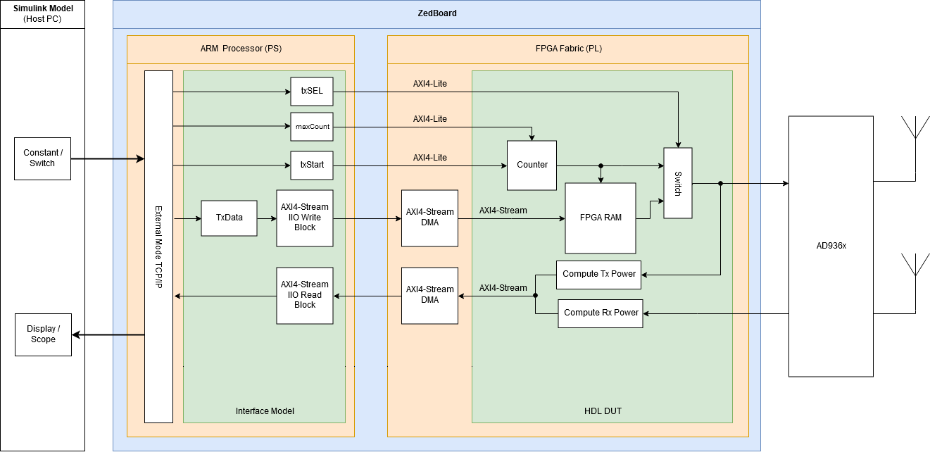
The HDL IP core has these port interfaces:
AXI4-Stream input ports for writing the waveform into FPGA RAM
AXI4-Stream output ports for reading the computed power of Tx and Rx signals into the PS
AXI4-Lite input ports for real-time control and adjustment of the design
AXI DMA ports for data movement of I/Q samples between the HDL IP core and the PS, via AXI DMA
Tx and Rx baseband ports for data movement of I/Q samples between the HDL IP core and the AD936x IP
The software interface model initializes the radio front end and controls the hardware model running in the PL. During execution of the model, the FPGA RAM is loaded with a chirp signal. At every trigger of the txStart register, the model sends the signal data to the AD936x radio front end for transmission and enables the receiver to capture the transmitted signal and any received signal over the air. The computed power (I/Q squared magnitude) of these signals is read from the PL into to the PS using the AXI4-Stream interface. The PS sends the received data to the host via UDP for real-time display.
Setup
To work with the HW/SW co-design workflow, you must install and configure additional support packages and third-party tools. For more information, see Installation for Hardware-Software Co-Design.
Hardware Generation Model
This Simulink® model is a hardware generation model using AXI4-Stream. From this model, you can generate HDL code for the PL and generate a template software interface model using HDL Workflow Advisor. Using the template software interface model, you can generate an application that runs on the PS.
The HDL_DUT subsystem models the functionality to be implemented on the PL. The highlighted blocks outside the subsystem represent the control functionality to be implemented on the PS. These have been modeled so you can verify behaviour via simulation.
modelname = 'zynqRadioHWSWAXI4StreamAD9361AD9364SL';
load_system(modelname);
open_system(modelname);
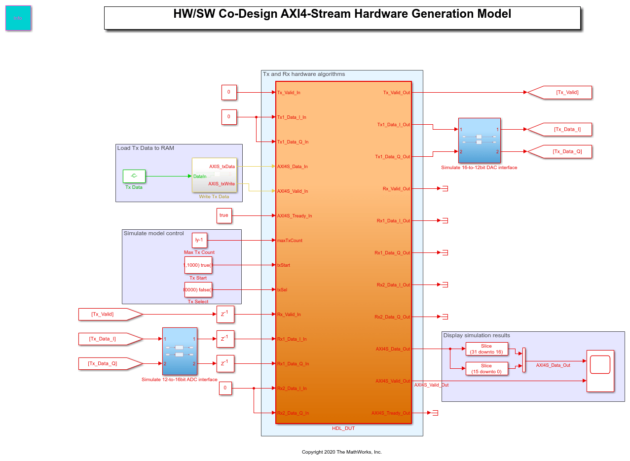
The Tx and Rx subsystems model the Tx logic and the Rx logic of the PL algorithm, respectively.
currentSubSys = 'HDL_DUT';
open_system([modelname '/' currentSubSys]);
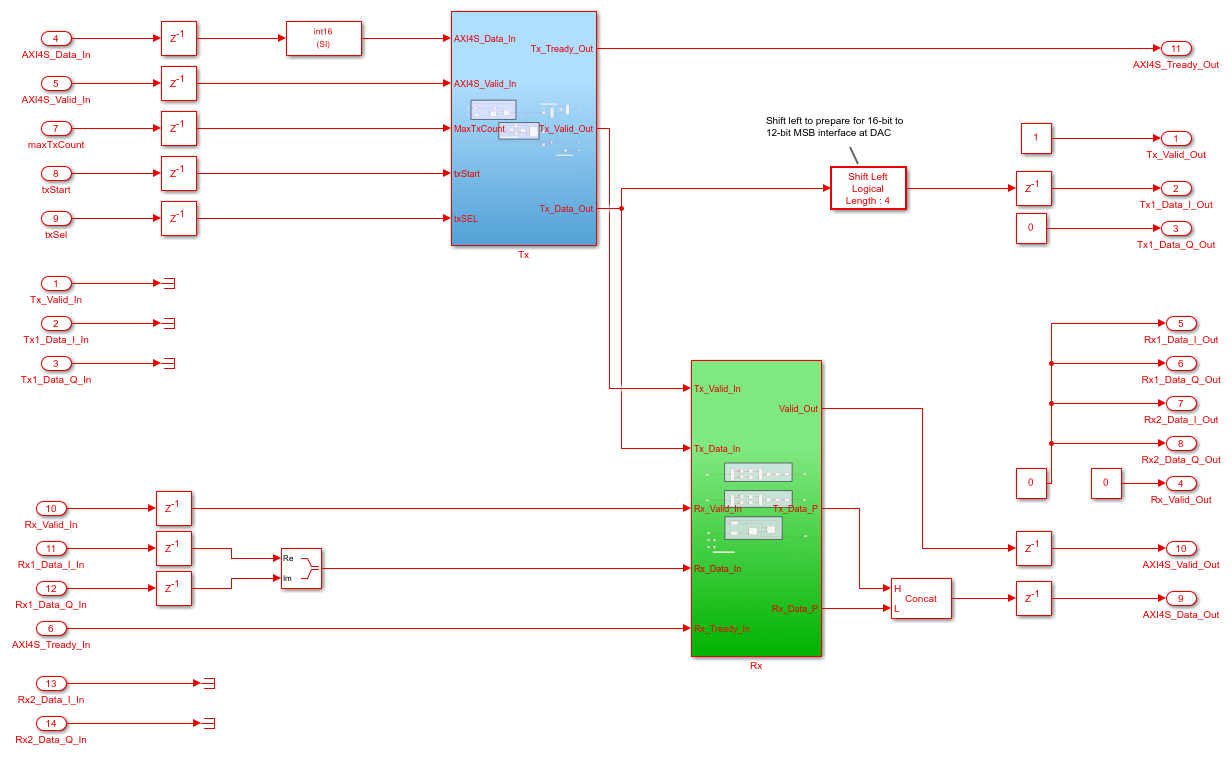
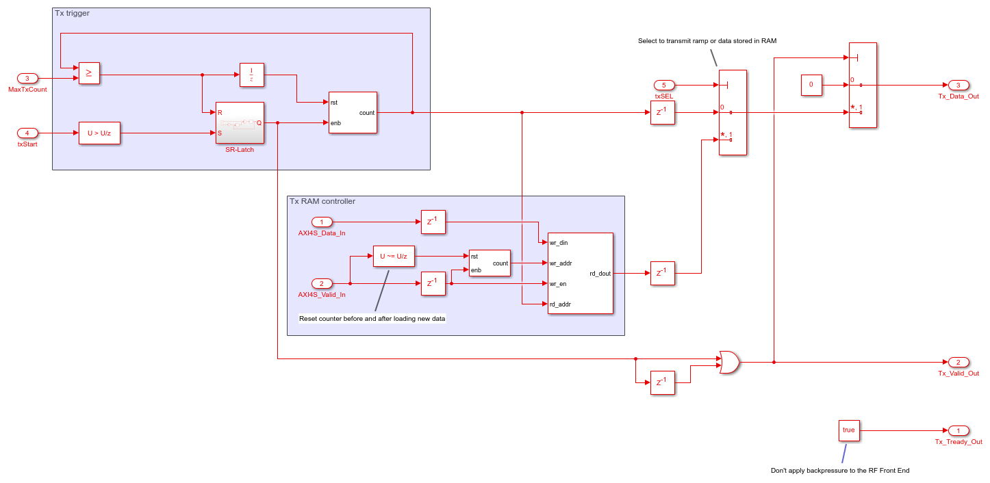
Within the Tx subsystem, a valid input frame of AXI4-S data is written to dual-port block RAM. Transmission of Tx data is controlled via maxTxCount, txSel and triggered via txStart.
currentSubSys = 'HDL_DUT/Tx';
open_system([modelname '/' currentSubSys]);
Within the Rx subsystem, the power (I/Q squared magnitude) is computed for both the transmitted and received signals. A Valid Out signal is generated, with valid period corresponding to 1.5x the frame size of the transmitted signal, in order to provide padding. This accounts for the time taken for the transmitted waveform to appear at the receiver.
currentSubSys = 'HDL_DUT/Rx';
open_system([modelname '/' currentSubSys]);
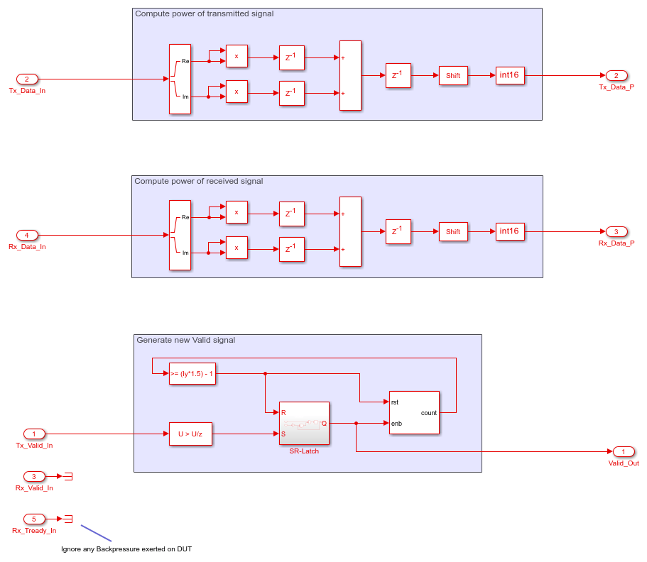
The HDL_DUT subsystem has designated ports that model AXI4 datapaths between the PS and PL.
AXI4-Lite registers:
maxTxCountdefines the maximum number of transmit signal samples (up to 2047).txStartwhen set to true triggers a single transmission ofmaxTxCountsamples.txSelswitches between transmitting data stored in the FPGA RAM by the PS or a ramp signal.
AXI4-Stream interfaces:
AXI4S_Data_Inloads Tx data from the PS to the FPGA RAM.AXI4S_Data_Outretrieves computed power of Tx and Rx signals to the PS.
Simulate Hardware Generation Model
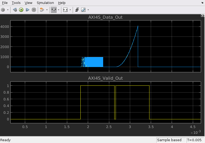
You can simulate this model to confirm its operation. A chirp signal is defined in workspace variable y. The signal is read into the model by the Tx Data block and scaled for representation by the int16 fixed-point data type. The Write Tx Data block generates AXI4-Stream Data and Valid signals, which are used to write the signal samples to RAM within the HDL_DUT subsystem. The AXI4-Lite control registers are modelled by the Max Tx Count, Tx Start and Tx Select blocks. The values of these blocks are configured to trigger a single transmission of the chirp signal, followed by a single transmission of the ramp signal, each for 2047 samples which is looped back over the I/Q interfaces. This transmission triggers a receive at the same time which allows both the transmitted and received signal to be captured for a certain length and the power of both signals are calculated before being transferred over the AXI4-Stream Data and Valid signals.
The simulation plots the power of the Tx and Rx data frames to the scope.
At this point you can start the process of generating the HDL IP Core, integrating it with the SDR reference design, and generating software for the ARM processor.
Generate IP Core
In preparation for targeting, you must set up the Xilinx tool chain by invoking the hdlsetuptoolpath function. For example:
>> hdlsetuptoolpath('ToolName','Xilinx Vivado','ToolPath','C:\Xilinx\Vivado\2019.1\bin\vivado.bat');
Start the targeting workflow by right-clicking the HDL_DUT subsystem and selecting HDL Code > HDL Workflow Advisor.
In Step 1.1, select
IP Core Generationworkflow and the appropriate Zynq radio platform:ADI RF SOM,ZC706 and FMCOMMS2/3/4,ZedBoard and FMCOMMS2/3/4,ZCU102 and FMCOMMS2/3/4, orZC706 and FMCOMMS5.In Step 1.2, select
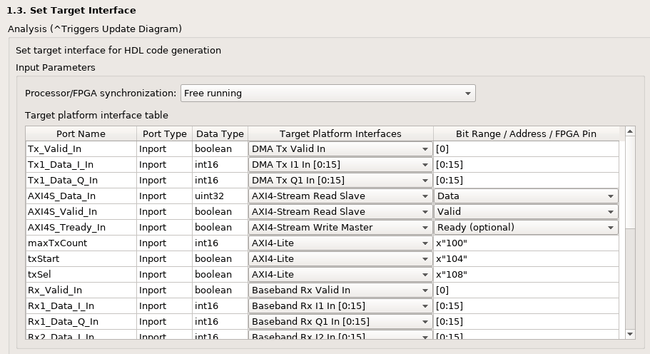
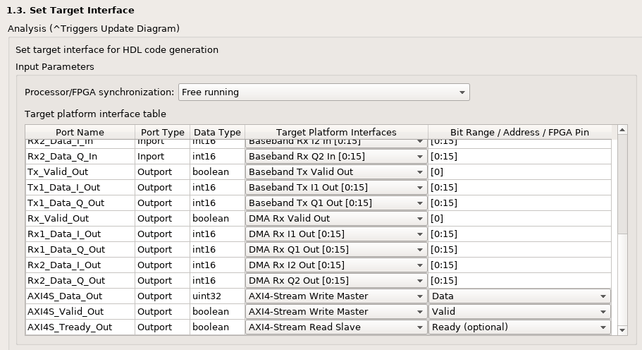
Receive and transmit pathreference design. For this example, you can use default reference design parameters.In Step 1.3, the interface table maps the DUT signals to the interface signals available in the reference design. For this example, configure the data and AXI4 interfaces as shown in these images.
In Step 1.4, set the DUT synthesis frequency. The DUT synthesis frequency depends on the baseband sampling rate of the system. In this example, the sample rate is 3.84 MHz, so a synthesis frequency of 4 MHz is sufficient.
Step 2 prepares the model for HDL code generation by performing design checks.
Step 3 generates HDL code for the IP core.
Generate Software Interface Model and Block Library
Step 4 of the HDL Workflow Advisor integrates the newly generated IP core into the Zynq SDR reference design, generates the corresponding bitstream, and loads the bitstream onto the board.
Step 4.2 generates a software interface library and a template software interface model.
Software Interface Library
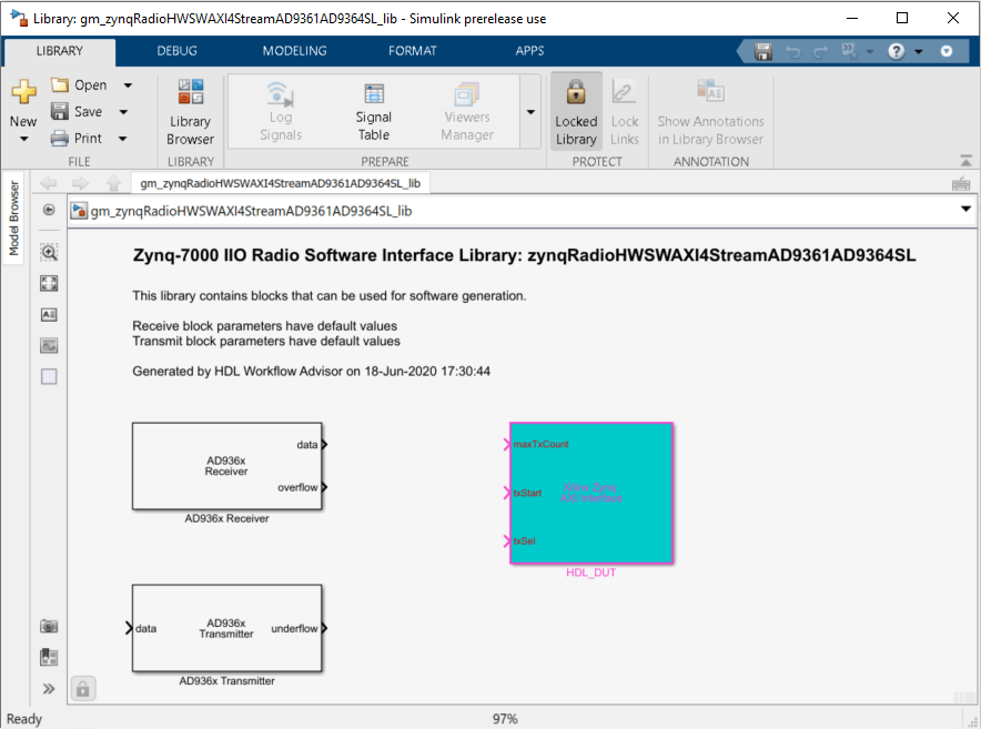
The library contains an AXI Interface block and radio blocks generated from the HDL_DUT subsystem.
The AXI Interface block exposes the AXI4-Lite control ports.
The data ports of the radio Receiver and Transmitter blocks represent the AXI DMA I/Q data interface between the FPGA user logic and the ARM processor.
AXI4-Stream driver blocks are not automatically added to the library. To use these in a model, you must manually add the AXI4-Stream IIO Read (Embedded Coder) and AXI4-Stream IIO Write (Embedded Coder) driver blocks from the Simulink Library Browser > Embedded Coder Support Package for Xilinx Zynq Platform library.
When using the software library blocks in a downstream model, you must configure the parameters correctly for your application. Take into account that any updates to the HDL_DUT subsystem are automatically propagated to the library blocks in the downstream model when you run Step 4.2 again.
Template Software Interface Model
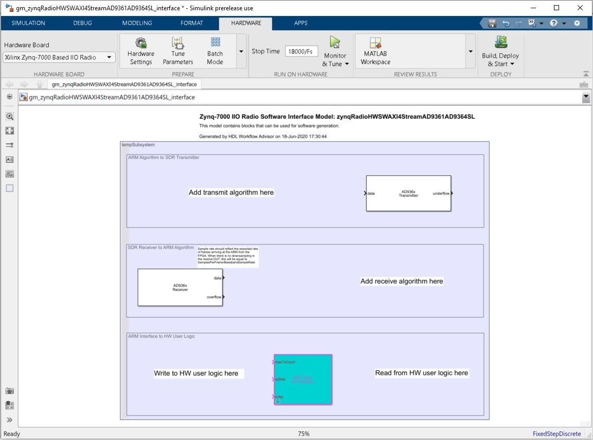
You can use the generated software interface model as a starting point for running your design on the Zynq with external mode simulation or full deployment. Since the generated model is overwritten each time you run Step 4.2, it is recommended that you save this model under a unique name and develop your software algorithm there.
Section AXI4-Stream Software Interface Model demonstrates how this generation model can be used to construct a software interface model that can run this example on the Zynq platform in Monitor & Tune mode.
Generate and Load Bitstream
The last steps of the HDL Workflow Advisor generate a bitstream for the PL and download the bitstream onto the board.
Step 4.3 generates a bitstream for the PL. You can execute this step in an external shell by selecting Run build process externally. This selection allows you to continue using MATLAB while building the FPGA image. Once some basic project checks are complete, Step 4.3 is marked with a green checkmark. However, you must wait until the external shell displays a successful bitstream build before moving on to the next step.
Step 4.4 downloads the bitstream onto the device. Before continuing with this step, make sure that MATLAB is set up with the correct physical IP address of the radio hardware by calling the
zynqfunction.
>> devzynq = zynq('linux','192.168.3.2','root','root','/tmp');
By default, the physical IP address of the radio hardware is 192.168.3.2. If you alter the radio hardware IP address during the hardware setup process, you must supply that address instead.
Alternatively, if you want to load the bitstream outside Workflow Advisor, create an SDR radio object and use the downloadImage function. The radio object to create depends on the radio platform selected in Step 1.1.
If the selected radio platform is either
ADI RF SOM,ZedBoard and FMCOMMS2/3/4,ZC706 and FMCOMMS2/3/4, orZCU102 and FMCOMMS2/3/4, create an AD936x radio object.
>> radio = sdrdev('AD936x');
If the selected radio platform is
ZC706 and FMCOMMS5, create an FMCOMMS5 radio object.
>> radio = sdrdev('FMCOMMS5');
Download the bitstream using the radio object interfacing the selected radio device.
>> downloadImage(radio,'FPGAImage', ...
     'hdl_prj\vivado_ip_prj\vivado_prj.runs\impl_1\system_top.bit')
     % Path to the generated bitstream
AXI4-Stream Software Interface Model
The AXI4-Stream interface model is developed from the generated template software interface model. The model allows you to run the algorithm in Monitor & Tune mode. In this mode, you can configure and trigger transmission and reception from the radio hardware in real-time.
close_system(modelname);
modelname = 'zynqRadioHWSWAXI4StreamAD9361AD9364SL_interface';
load_system(modelname)
open_system(modelname)
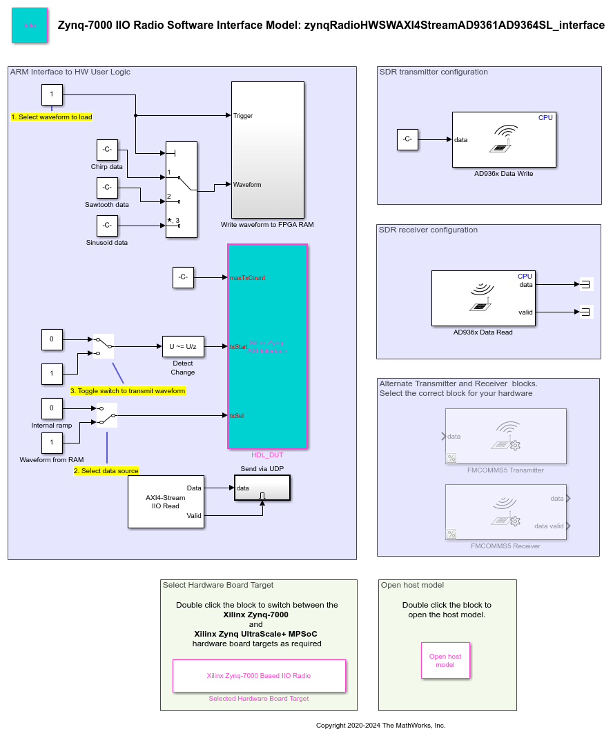
The model has been configured to run using the Xilinx Zynq-7000 Based IIO Radio target. You can use this target for the ADI RF SOM, ZedBoard and FMCOMMS2/3/4, ZC706 and FMCOMMS2/3/4, or the ZC706 and FMCOMMS5 radio platforms. If you are using the ZCU102 and FMCOMMS2/3/4 radio platform, double click the Selected Hardware Board Target block to change the configuration to use the Xilinx Zynq UltraScale+ MPSoC ZCU102 IIO Radio target.
The AD936x Data Write block initializes RF parameters and enables the transmit data path. This block must be included in the interface model, even though the block does not send any data from the PS to the PL.
The AD936x Data Read block initializes RF parameters and enables the receive data path. This block must be included in the interface model, even though the block does not receive any data from the PL.
The AXI4-Stream IIO Read (Embedded Coder) and AXI4-Stream IIO Write (Embedded Coder) driver blocks have been added to the interface model from the Simulink Library Browser > Embedded Coder Support Package for Xilinx Zynq Platform library and configured for the example, as outlined in Generate IP Core with AXI-Stream Interface (HDL Coder). The AXI4-Stream IIO Write block is used in the Write waveform to FPGA RAM triggered subsystem to write the waveform from the PS to the PL. The AXI4-Stream IIO Read block is used to read the received power signal from the PL to the PS, then send it to the host via the Send via UDP subsystem.
For more information on software interface model configuration, refer to Guidelines for Configuring the Software Interface Model
Run Design on Zynq Board
During model execution, you can control the transmission of the signal by following 3 steps, as outlined in the highlighted annotations in the interface model
1. Signal Select selects the waveform data and loads it into FPGA RAM.
2. Switch Source toggles transmission signal between the loaded waveform or a ramp signal.
3. Trigger triggers a single transmission of the signal to the radio front end.
Once the PS has successfully received an AXI4-Stream transaction, it sends the frame of data to the host over the Ethernet cable using the UDP send block in the software interface model. The UDP send block has been configured using the default IP address of the host '192.168.3.1'. If you altered the radio hardware IP address during the hardware setup process, you must supply the corresponding host address instead. A simple UDP receive model has been supplied which you can use to receive and display the frame data in real time using the scope block.
close_system(modelname);
modelname = 'zynqRadioHWSWAXI4StreamAD9361AD9364SL_UDP_host_interface';
load_system(modelname)
open_system(modelname)

1. Run the UDP receive model
2. Run the software interface model in Monitor & Tune mode
3. Double click the Trigger switch in the software interface model to transmit the selected waveform and trigger the receive.
The received power signals appear in real-time on the Scope in the UDP receive model.
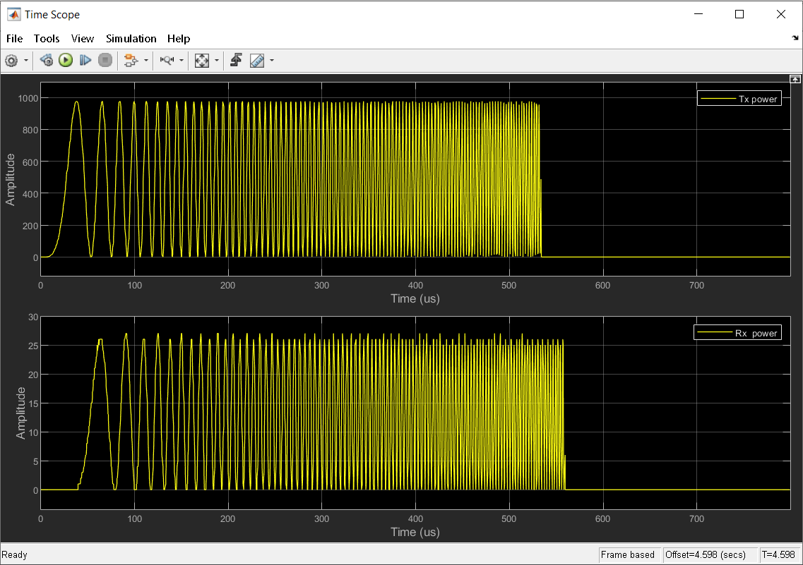
The frames of data displayed in the Scope block of the UDP receive model correspond to the power (I/Q squared magnitude) of the plotted signals. This matches the functionality of the simulation model.
This result is captured using an RF antenna attached to the transmit and receive ports of the hardware, you can change the power of the received signal by modifying the Gain (dB) value on the AD936x Data Read block mask.
Summary
This example shows you how to use the AXI4-Stream interface with the Analog Devices AD9361/AD9364 radio by implementing, simulating, and deploying a simple triggered waveform transmitter and receiver on the hardware.
close_system(modelname);