Detect PCB Defects in Live Image Stream Using Visual Anomaly Detector
R2026bThis example shows how to detect and localize defects on printed circuit board (PCB) images in a live image stream using a trained anomaly detector in the Visual Anomaly Detector app.
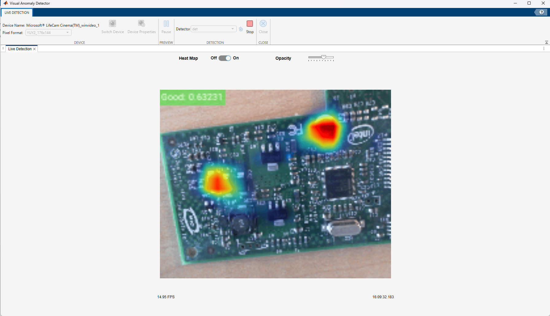
In a production environment, PCBs move along a conveyor belt and pass under an inspection camera. Using Visual Anomaly Detector app, you can connect to the camera, run inference on each captured frame using a trained anomaly detector, and visualize detection results in real time. Each frame is annotated with a classification result (Good or Bad) and an anomaly score. You can also enable an anomaly heatmap overlay to localize defects at the pixel level.
This example requires Image Acquisition Toolbox™, a trained anomaly detector in the MATLAB base workspace, and a supported camera connected to your system. You can train a detector using Visual Anomaly Detector app, or programmatically using training functions. For an example on how to train a detector using the Visual Anomaly Detector app, see Train and Evaluate Anomaly Detection Model Using Visual Anomaly Detector. For an example on training a PatchCore detector on PCB data, see Localize Industrial Defects Using PatchCore Anomaly Detector.
Open App and Connect to Camera
Open the Visual Anomaly Detector app. On the MATLAB Toolstrip, select the Apps tab. Then, in the Image Processing and Computer Vision section, click Visual Anomaly Detector. Alternatively, open the app programmatically.
visualAnomalyDetector
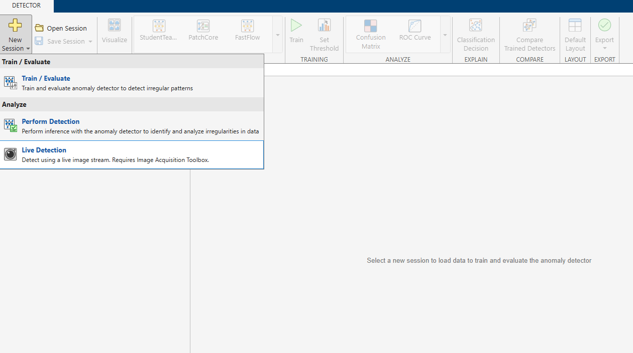
On the Detector tab of the app toolstrip, click New Session, and then select Live Detection.
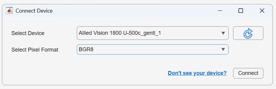
In the Connect Device dialog, select the connected camera you want to use from the Select Device dropdown, and then choose the desired pixel format from the Select Pixel Format dropdown. Click Connect to establish the connection.
If the app does not detect your camera, click the Don't see your device? The app opens a troubleshooting page with information about required support packages, driver installation, and other configuration steps to help the app recognize your device. For more information on troubleshooting tips, see Troubleshooting in Image Acquisition Toolbox (Image Acquisition Toolbox).
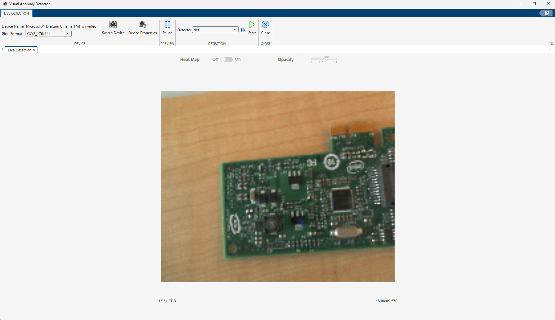
After a successful connection, the app opens the Live Detection tab.
Preview Live Image Stream
Before running detection, verify that the camera is capturing the PCB images correctly. In the Device section of the toolstrip, click Preview to start a live preview. The app displays the live image stream along with the current frame rate (FPS) and a timestamp at the bottom of the preview. Use the preview to confirm that the PCBs are positioned correctly within the field of view and that the image quality is adequate for defect detection. Click Preview again to pause the stream.
Adjust Device Settings
To adjust the camera settings, use the Device section of the toolstrip. To switch to a different connected camera, click Switch Device and select the new device. To change the pixel format, use the Pixel Format dropdown.
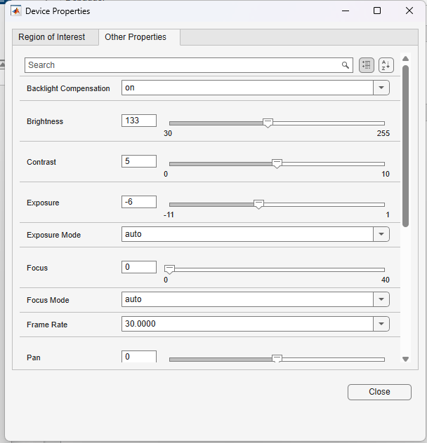
To change the captured region or resolution, click Device Properties. The properties panel opens on the right side of the app. Select the Region of Interest tab to adjust the X Offset, Y Offset, Width, and Height of the captured area. Click Apply to confirm your changes, or Reset to revert to the default values.
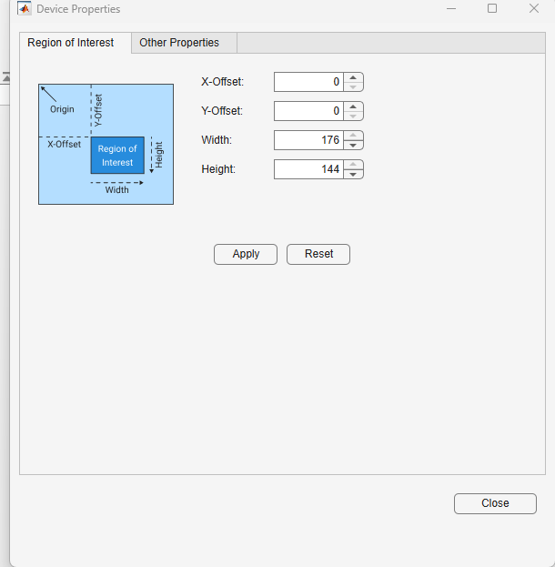
To fine-tune image quality, select the Other Properties tab in the properties panel. This opens a property inspector where you can configure device-specific settings such as Exposure and Gain. Adjust these parameters to optimize the image for more reliable defect detection.
Select Trained Detector and Start Detection
Once you are satisfied with the preview, select the anomaly detector you want to use for inference on live image stream. In the Detection section of the toolstrip, click the Detector dropdown and choose a trained detector. This dropdown lists all anomaly detector objects that are currently loaded in the MATLAB base workspace. If you have recently trained or loaded a detector and it does not appear in the list, click the Refresh button to reload the workspace.
Click Start to begin live anomaly detection. The app runs the selected detector on each incoming frame and annotates the image with the detection result. A green label showing Good followed by the anomaly score indicates that the PCB passed inspection. A red label showing Bad followed by the anomaly score indicates that the detector has identified a potential defect. The anomaly score is a numeric value where higher scores indicate a greater likelihood of a defect.
Enable Anomaly Heatmap Overlay
To localize defects at the pixel level while detection is running, toggle the Heat Map switch to On in the document area. The app overlays a color-coded heatmap on each frame, where warmer colors indicate a higher probability of anomaly at each pixel location. This helps you visually identify the specific regions on the PCB where defects such as scratches, missing components, or solder issues are located.
To adjust the visibility of the heatmap relative to the underlying PCB image, use the Opacity slider. Move the slider to the right to make the heatmap more prominent, or to the left to let more of the original image show through. By default, the heat map is off and the opacity is set to a moderate value.
Stop Detection and Close
When you are done inspecting, click Stop in the Detection section to end live anomaly detection. The app stops running inference and returns to the idle preview state.
To close the Live Detection tab and return to the main Detector tab, click Close in the Detection section of the toolstrip.

