Vias
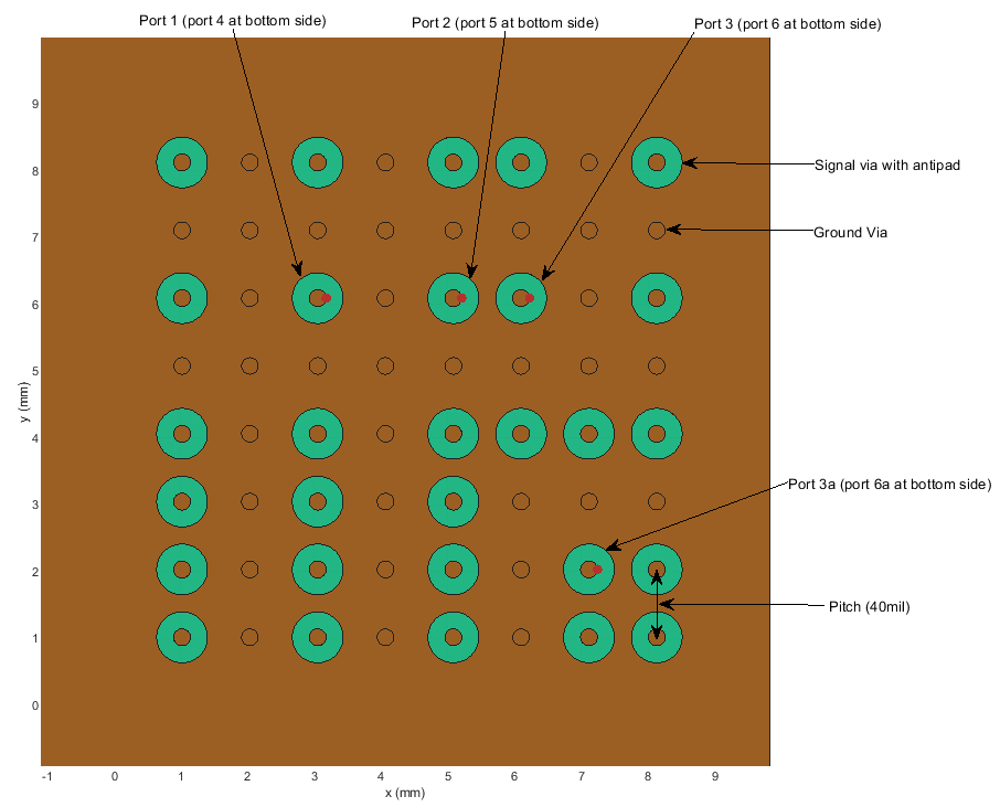
Vias (vertical interconnect access) are an essential part of a multilayered PCB (printed circuit board) design. Vias make an electrical connection between the different layers of a PCB. These are constructed by placing copper pads on each layer of the PCB and drilling a hole through them. The inner part of the via, is filled with a non-conductive material, and the outer layer are coated with a conductive plating used to connect each layer in the PCB.
Objects
viaSingleEnded | Create single ended via in PCB stack (Since R2023a) |
Functions
show | Display PCB component structure or PCB shape (Since R2021b) |
shapes | Extract all metal layer shapes of PCB component (Since R2021b) |
gapratedistance | Gap rate distance metric (Since R2023a) |
criticalwavelength | Number of wavelengths between signal via and ground return vias (Since R2023a) |
padsTable | Display pad stack used by viaSingleEnded in a table (Since R2024a) |
antipadsTable | Display antipads stack used by viaSingleEnded in a tabular
from (Since R2024a) |
getpads | Generate a pad stack (Since R2024a) |
getantipads | Generate antipad stack (Since R2024a) |
Topics
- Eigenmode-Based Solver for PCB Vias
Wave generation and propagation in vias, circuit model, equations.
Featured Examples

Single Ended Via Analysis with Placement of Ground Return Vias for 40+ Gbps Signaling
Model the return path of single ended printed circuit board vias using the viaSingleEnded object.
Managing Differential Via Crosstalk and Ground Via Placement for 40+ Gbps Signaling
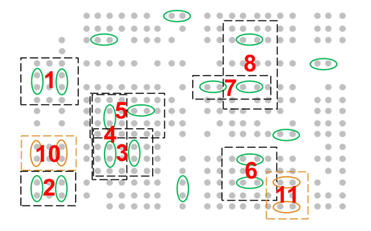
Model the crosstalk of differential signal vias (DSVs) using the via analysis feature in RF PCB Toolbox viaSingleEnded to ensure robust signaling over 40 Gbps. DSVs are subject to crosstalk phenomenon shown in [1] because crosstalk is induced by waves propagating among the Ground Return Vias (GRV) planes and patterns and is less related to the signal return path concerns that affect signal loss and impedance. GRVs do not form a shield around a given site on a PCB at higher frequencies because GRVs do not stop energy propagation; they simply reflect or deflect it. And, based on physical dimensions and materials, this reflected energy may resonate.
Modeling of via array with open signal vias
Modeling of a via array containing open signal vias [1]. Variation of pitch (distance of the via array grid) and variation in the number of board layers is studied.